
A cheap
and easy all HF bands tranceiver
designed by sv3ora
This
transceiver is a successor to my all
bands receiver. To find out how the receiver portion of the
transceiver works, follow this link.
Here, the modifications to the receiver to convert it to a transceiver,
will be presented. All the versions will be presented sequentially,
along with their modifications, as a timeline of the progress and as a
way for you to choose which version of the transceiver to build.
 |
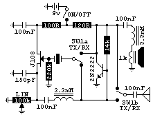
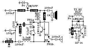
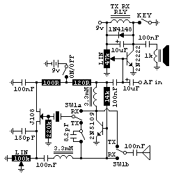
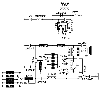
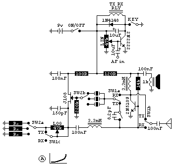
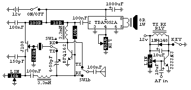
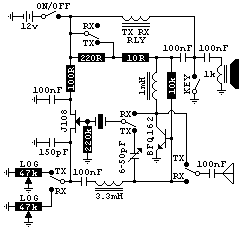
The first version of the transceiver, uses the preamplifier as an RF amplifier as well. SW1, is the key and switches between TX and RX. It also takes care of the TX/RX offset in this configuration. The key is shown in the TX position in the schematic. Note the change in the BJT type (compared to the original receiver) and the collector and base resistors, to achieve maximum power output and also minimum harmonics. Power output is about 5mW at 50R. All harmonics are about 50dBc! |
|
|
|
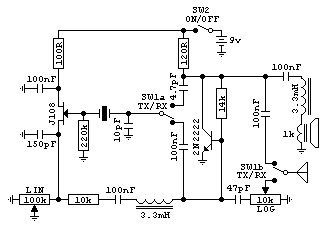 |
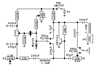
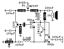
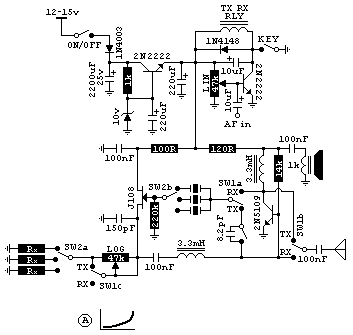
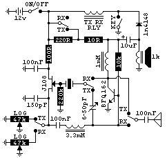
The second version of the transceiver is shown on the left image. This time, it does not use a varactor at all, which make the transceiver even easier to build. I found that when using crystals, the varactor has little effect on the TX offset. Even without the varactor in place the TX offset was at maximum and at LSB. The TX offset is primarily affected by the 100nF TX coupling capacitor near SW1a and the capacitance of the BJT. Practically, the varactor has an effect in setting the RX offset, or frequency if you like. To keep things simple I kept the Rx frequency fixed (set by the crystal and the 10pF) and the TX ofset at maximum amount at all times. This TX offset amount is is not fixed but depends on the band of operation. On 10m the offset is about 2KHz, on 40m about 1KHz and on 80m a few 100s of Hz. On 160m and 80m the offset is too low. If you find this unnoying, add or remove capacitance during TX/RX accordingly on these bands. Thankfully, the human ear can easily listen tones of up to 6KHz or more between noise, so the non-variable offset was not considered a big problem during practical operation. After all the crystal/varactor offset is small and it also depends on band of operation. Instead of the varactor there is a fixed 10pF capacitor to the ground, which helps oscillation in high frequencies. Because this is small, it has less effect during RX, so it should attenuate RX signals less. |
|
|
|
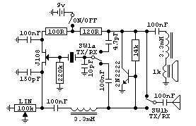 |
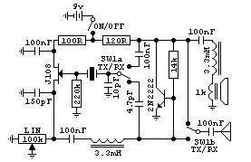
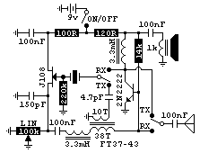
The third version of the transceiver is shown on the left image. In this version I did more simplifications. I removed the input attenuator. We are trying to maximize sensitivity and because of the low input signals involved and without any more audio amplification, the input attenuator has no real meaning as it is almost always set to maximum. The attenuator has a meaning only to attenuate very strong out of band broadcast signals so as not to get rectified in the 2n2222 B-E junction which acts as a crystal receiver that way. Then you increase the audio amplification to receive only the wanted signals. But this RX has no extra AF amplifiers, so the input attenuator is almost always set to maximum. Removing the input attenuator makes possible to remove its 47pF coupling capacitor too. But to DC isolate the antenna, I connected the 100nF capacitor directly to it and I removed the other two 100nF and 47pF from the TX and the RX respectively. The extra capacitance during RX may yeld in greater sensitivity or lower frequency response. The most important modification was the removal of the 10k fixed sourse resistor. This has a huge impact, it increased the audio volume out of the receiver many times! Now the receiver is very sensitive using crystals. |
|
|
|
 |
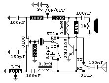
The
fourth version of the transceiver is shown on the left image. This time
I switched the
places of the 100nF and 4.7pF capacitors. This had a huge impact on
receiver, it increased
the audio volume out of the receiver many times! Now this is a
really sensitive receiver and I can even hear things using low
impedance phones, although this is not nominal. This change, changed the direction of the TX offset. Now the local oscillator is below the TX signal, so the TX is in USB now and not in LSB as before. This is great because I now can set the receiver to single signal USB operation (rejecting the LSB) and the TX is also in the USB. However this comes with a disadvantage. The TX power is reduced quite a lot, because now, the coupling from the local oscillator to the TX amplifier is only 4.7pF, instead of 100nF. We cannot change the value of the 4.7pF because this would also change the offset. With this change, I noticed that the offset improved a bit at lower bands, now I can operate on 160m, although the tone is low, but it is distinguishable. |
|
|
|
 |
The fifth version of the transceiver is shown on the left image. I realized that the 100nF and 4.7pF capacitors near SW1a were not needed for DC isolation, because the crystal will block DC anyway. Because the crystal "sees" the maximum shunt capacitance of the BJT in this configuration (direct coupled both in TX and RX), the 10pF ia also not needed. The TX power is maximum now, however in this version there is no TX/RX offset. I will figure out how this can be done in the next version, and some of the capacitors may be reinserted to the circuit. So this version is not final. |
|
|
|
 |
The sixth version of the transceiver is shown on the left image. I have changed the position of the inductor, placed it in a more appropriate place. The change in the inductor position had desired effects. First, it raised the output power a bit. Not too much but just a bit (1-2dBm), especially on lower bands. On higher bands there was no difference in output power. More importantly, this inductor also caused the oscillator frequency to get lower, thus there is some TX/TR offset now in the wanted direction (TX on USB). On 10m the offset is around 1KHz (be ear), so this was worth the effort. I believe that the inductor there will also help to better isolate the DC line of the oscillator and the RF amplifier, although I cannot test this. There was no audible difference in RX (as far as I can remember from the previous version). |
|
|
|
 |
The
seventh version of the transceiver is shown on the left image. Since we
want the LO
on TX to be at a higher frequency for USB operation and at the same
time maximum sensitivity on RX, we want maximum capacitance present on
the resonator on RX and lowest capacitance presented on the resonator
on TX (for the offset setting). However, at the same time we want to
maximize power transfer from the oscillator to the BJT amplifier during
TX, so a single small coupling capacitor, whereas it achieves the
desirable offset, cannot couple enough power to the amplifier. The
problem could be solved with magnetic coupling. A transformer,
connected as shown in the schematic achieves that. The
small capacitor in series with the TX switch, ensures minimum
capacitance presented to the oscillator resonator during TX. The
step-up transformer ensures the low coupled voltage from the capacitor,
will be stepped-up again. The secondary of the transformer, provides a
low impedance to the audio during RX (let it pass through it). I have not yet tested this configuration on RX. I have tested it on TX. It achieves the desirable maximum offset and the output power at all bands, except 10m, where the output is low and 180m, where the oscillator does not start. So I need to test and optimize the circuit further. |
|
|
|
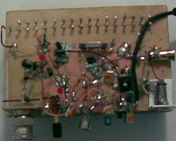
 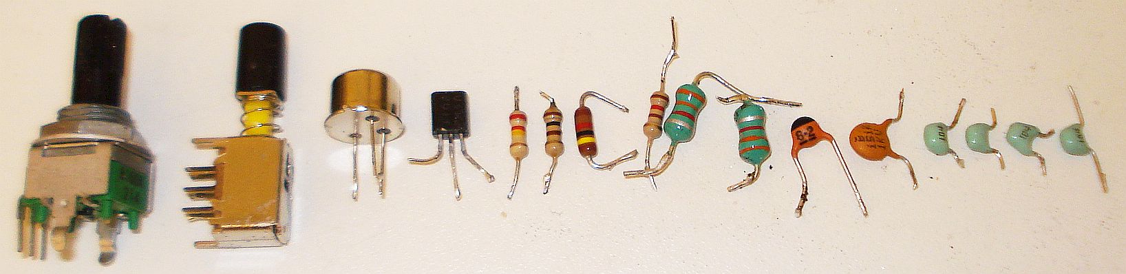 All the components needed |
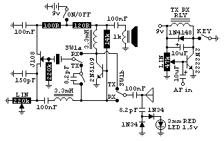
The
eight version of the transceiver is shown on the left image. I found
that the transformer option for the offset did not work very well. So I
tested different BJTs and I finally used the 2n5109 which provided a
bit more gain. This allowed a relatively low value capacitor to be
placed in series (8.2pF) to achieve enough offset at the lower bands
and the output power could be still set to 7dBm. At 40m and above, the
offset is too high with this capacitor in series, so a SPST switch
short circuits it. I would like to avoid having another switch, but I
am affraid this is the price to pay for non using a variable offset
tuning using a varicap or a capacitor. An interesting thing of the series capacitor is that the harmonics improved in the 80m band. Now they are at -37dBc at 80m. At 40m they are about -42dBc and at 10m at -40dBc. The harmonics performance on 160m is only -17dBc. These readings were done with the output power set at +7dBm (~5mW) at 50R at all bands. |
|
|
|
 |
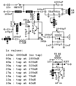
For
those of you who want to connect the transceiver to the PC, here is a
suitable automatic keyer I have designed. This keyer operates from
sound tones
out of the PC sound card (convenient in modern laptops) and it uses the
lowest amount of
components. If you use a relay that has an internal diode embedded, the
1n4148 diode is not needed. If you are absolutely sure that your sound
card is DC isolated, then the input 10uF capacitor is not needed too. The keyer works in a totally different way than the clasic voltage doubler and transistor circuits. Here, the transistor works as an AF amplifier, amplifying audio out of the sound card without rectifying it, so that to make the circuit really sensitive in a single stage. The trimmer resistor must be set so that the relay is switched off, just before it starts to switch on. This adjustment must be done only once, with no audio signal applied to the keyer. Make sure you never set the wiper of the trimmer close to the 9v, because you will damage the potentiometer! If the keyer is set as described above, then an audio signal from the PC, will give it the extra boost needed to switch the transistor on, or more precisely to switch the relay on. However, the operation of the circuit in that way, causes the relay to pulsate at the rate of the audio signal. To prevent this, a 10uF capacitor is used across the relay coil. The automatic keyer operates from only 30% of the volume on my laptop sound card, which is something that can't be achieved by other single transistor keyers without voltage doublers or step up transformers. It operates reliably from about 100Hz to 3KHz of audio tone. It is tested to operate on CW 5WPM to 25WPM without problems. |
|
|
|
 |
With
the addition of the automatic keyer, the manual key goes away. If you
want both the automatic keyer and a manual key to be present, you can
connect your manual key between the 2n2222 collector and the ground.
The key shorts the transistor and connects the relay coil directly to
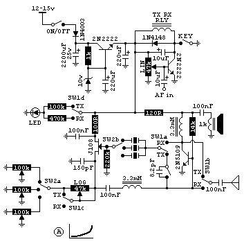
the ground, energizing it. For the manual key, you can use an external key of your choice, or an embedded key as before. In the case of the embedded key, this can be a single SPST switch. Note in the schematic on the left, I have changed the regeneration potentiometer to 220k, to be able to receive AM also on 40m (allows setting below the oscillation threshold), which was problematic before. Below is the first real test I did with slow-hell mode on 10m. The transceiver was connected to a PC running fldigi in slow-hell mode, in another room about 10 meters away and a CB rubber duck was attached to it. The receiver was a 10m SSB handheld in the other room, placed close to the other PC microphone (not physically connected to the PC). I varied the audio volume of the handheld continuously and I did several other noises that were picked by the microphone as well as the slow-hell tone. This hopefully simulates a noisy HF band. |
 |
|
|
|
|
 |
In
this version i tried to use the keyer as an audio amplifier on RX. This
should give even greater audio output. I have tested it though and it
did not work as expected. The audio amplification at the best case
(setting of the 47k trimmer) was the same as without this extra stage.
However, this setting was not the optimal for the keyer operation. I
believe the optimum keyer bias was not the optimum audio amplification
bias. Also, this version gave annoying clicks on the headphones, when
the manual key was closed. I may try optimizing this version in future time, so I leave this experiment here. For the time being, I will stick with the previous version, which works as expected. |
|
|
|
 |
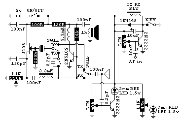
When
you have a spectrum analyzer near by, it is easy to set the
regeneration potentiometer so that the output power of the transmitter
is +7dBm and so that the harmonics to be kept at minimum. However, in
the field there is not such a luxury. To overcome the problem a very
simple power monitor has been added to the transceiver. When inserting a new crystal, close the key to transmit and set the regeneration potentiometer so that the LED is just switched off. In fact, you have to set it a bit more in the off state, as the LED is completely switched to off at +9dBm and below. So turn the pot a little bit more to lower down the output power a bit more. Note that you have to ensure that the LED is completely off, as at it's lower settings it is dim, but not actually switched off. You have to use a 1.5mm red led that operates at 1.5v. This is important, do not use another color, size or voltage LED. The diodes can be any germanium small signal diodes. The power monitor circuit has been tested at all bands and has the same behaviour. It does not affect the output signal neither on harmonics performance nor at power output. The small coupling capacitor is important in that sense. |
|
|
|
 |
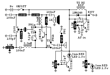
Here
is a new version of the transceiver. The only thing
that has been changed, is the power monitor circuit. The previous power
monitor had the disadvantage that you should tune the LED to be off
during TX. Also, you should tune the LED a bit more to the off side
(without being able to monitor it), to reach the +7dBm level by
guessing. This version, without adding more components, uses a
transistor to drive the LED, making it more sensitive. Another
advantage of this version, is that the led turns on during TX, so it is
used as a TX RF power indicator as well. Actualy, the brightness of the
LED changes, it does not swithed off completely. Calibration of the trimmer at the base of the transistor is a one-time process and it is easy. With a 50 ohm spectrum analyzer connected at the output of the transmitter, tune the regeneration potentiometer so that the output power of the transmitter (excluding harmonics) is +7dBm. Then tune the 47k trimmer at the base of the transistor in the power monitor circuit, so that the LED is turned on. Do not make the LED neither too bright nor too dim, but find about a middle brightness point, maybe a bit on the dim side, it is up to you really. Make sure you never set the wiper of the trimmer close to the 9v, because you will damage the potentiometer and the LED! Start with the wiper at the ground point just to be safe. If a spectrum analyzer is not available, calibration of the power monitor can be done with a harmonics-free +7dBm signal generator, connected to the power monitor circuit alone during calibration. For just two extra components, you can have a simple RF power calibrator, without the need for a spectrum analyzer or an external oscillator any more (after the initial calibration of the power monitor described previously of course). An extra trimmer resistor is used, to set the brightness of an identical LED with that of the power monitor (same type and brand, just buy two of them), to the same level as that of the power monitor LED. Just tune the trimmer in this calibrator so that it's LED has exactly the same brightness as the LED of the power monitor during TX. Like previously, make sure you never set the wiper of the calibrator trimmer high, because you will damage the LED! Start with the wiper at the ground point just to be safe. Every time you insert another crystal to the transceiver you just tune the regeneration potentiometer during TX, so that the brightness of the power monitor LED is the same as the brightness of the calibrator LED. The calibration LED is also used as a power-ON LED for the transceiver, since it stays ON all the time during the operation of the transceiver. A note, the system assumes a 50 ohm antenna to be connected to it. Other impedances will not give correct power monitor readings while the calibrator has been set for 50 ohms. |
|
|
|
  |
This
version uses a 47 ohm resistor (can be two 100 ohms in parallel) and a
momentary switch (SW2). The resistor acts as a dummy load when the
momentary switch is pressed. Of course the antenna must be disconnected
when doing so. The purpose of the resistor is to present a 50 ohm load
to the transmitter so that the power monitor LED can be set to the
correct brightness with the regeneration potentiometer. Set the
transceiver to transmit and close the SW2 with the antenna
disconnected. Then adjust the regeneration potentiometer a
described previously. |
|
|
|
   |
In
this version of the transceiver, I have removed the power monitor and
the rest of the components related to the resetting of the regeneration
potentiometer when a new crystal is inserted. This greatly reduces the
amount of components needed. It also allows you to have your crystals
permanently connected to the transceiver, so that you do not have to
carry them with you. I did this, thinking that the shortwave in-band
crystals that you are likely be able to find, won't be more than a few
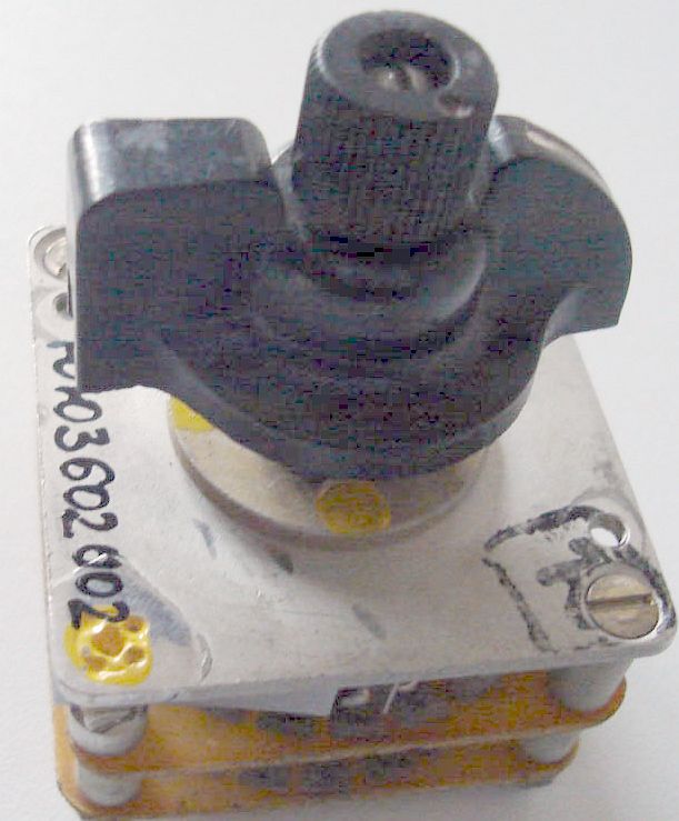
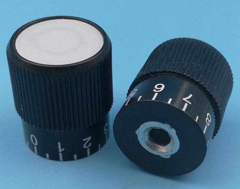
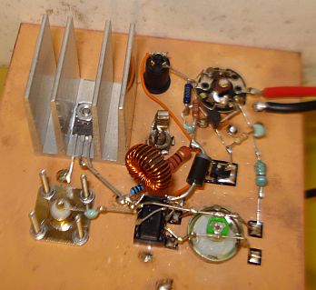
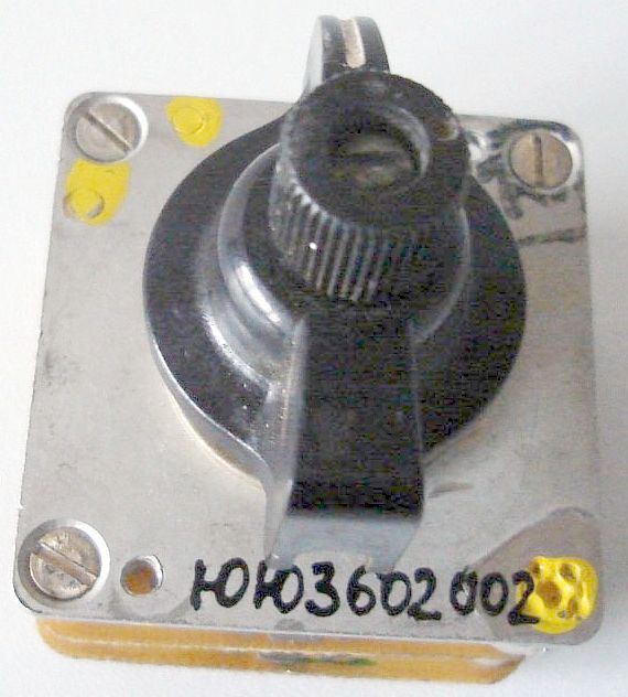
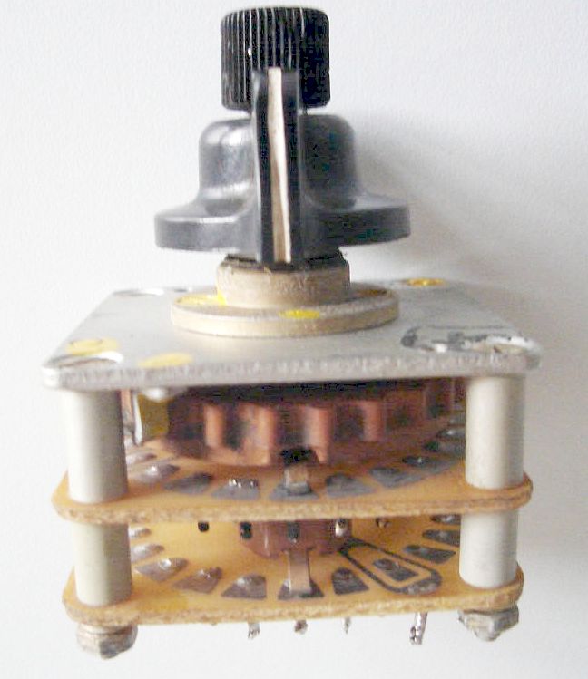
dozen at best case. Here, a 2-pole multi-position selector switch is used to select each crystal and at the same time to preset the correct regeneration for that particular crystal. Therefore, each time you turn to another crystal, the regeneration will be set to the optimum point for that particular crystal. A 2-pole 5-position switch is shown in the schematic, but you can use any number of positions, the bigger the better. Just have in mind that as the number of positions is increased, the switch gets bigger and more expensive or even rare to find. In my case, I was lucky to find a Russian millitary switch of 2-poles and 24-positions at a good price (photos 1, 2, 3, 4). However, there are many cheap Chineese 24-position switches, sold at low prices online. Solder all of your crystals onto the selector switch, set Px for zero ohms and then for each crystal you select, place the right amount of resistance (Rx) so that the RF output level on transmit is 5mW at 50 ohm. Rx can be a fixed resistor, a combination of resistors in parallel or in series, or it can be a small trimmer which is set for the right amount of resistance. When everything is set up correctly, with Px set at zero ohms, the TX output power will be 5mW at 50 ohm for each crystal frequency and the harmonics will be kept to minimum. With Px at zero ohms, the oscillator/detector will always oscillate (DSB reception) and it's RF level will be such, so as to satisfy the 5mW of TX output power. As you increase the value of Px, the TX output power decreases, but at some point wou begin rejecting the LSB, receiving only the USB. As you continue to increase the value of Px, you then receive AM. Of course the output power of the transmitter is affected by the setting of Px at all these cases. Here is a nice knob I found for Px. The amount of crystals that the circuit can accept, is only limited by the capacity of the selector switch. If you can't purchase switches online, visit your nearest electronics shop and ask for a stereo selector switch. These are very common because they are used as stereo signal selectors in audio preamplifiers. |
|
|
|
 |
In
this version, there are several differences from the previous one.
First, I have drawn only three crystals and Rx resistors, just to make
the schematic diagram cleaner. You can understsand the way more
crystals can be connected to the circuit anyway. The next change, was to use an extra switch (SW1c) that short circuits the potentiometer at the source of the JFET during TX. The previous version of the schematic had problems, in the sense that when you preset Rx for an output of 5mW out of the transmitter, Px must be set for zero ohms to retain the output power on TX. But this did not give any adjustability on RX. In other words you could either transmit 5mW and regeive DSB only, or force the reduction of the TX power, if Px was to be set in any other value, like when setting it for USB only operation. In this version, with the use of SW1c, the TX and RX work independently and you can set the regeneration potentiometer at any value you wish during RX, without affecting the output power during TX. Since SW1c short circuits the regeneration potentiometer during TX, the TX output power is only defined by the setting of the resistor Rx and not by the setting of the potentiometer. With the addition of SW1c, a quad relay is required in the circuit for SW1 (I am not aware of any triple relays that is why I say quad). Quad relays are harder to find, but I happened to have a few. However, if you cannot find one, don't get dissapointed. You can use two dual relays in series to create a triple relay switch. The coil of the first relay will be connected to the keyer circuit and one of it's switches will be SW1c. It's other switch is connected to 9v at one side and to the coil of the second relay at the other side, so that when the first relay is energized, it also energizes the second relay. The two switches of the second relay will be SW1a and SW1b. The last change I did to the circuit was the replacement of the linear regeneration potentiometer with a logarithmic one. I found the previously used linear potentiometer to be more difficult to set (touchy) at higher bands, especially on 10m. The use of a logarithmic potentiometer can cure this to some extent. Take care of how you will connect this potentiometer to the circuit, this is important. I have drawn a small graph with the logarithmic scale (marked as "A" below the potentiometer), to help you on this. The logarithmic scale you see on this graph must match the potentiometer above it. That is, when you bring the wiper of the potentiometer right at the middle setting of the potentiometer, the resistance you measure from the wiper to the left side (the one connected to Rx) must be much smaller than the resistance to the right side (the one connected to the 100nF). This is how you can find the proper way of connecting the potentiometer. |
|
|
|
 |
This
version is identical to the previous one, except that I have added a
suitable regulated power supply to it, so that the battery can be
eliminated in non-portable operation. After all, the transceiver draws
about 30mA continuously and this can drain the 9v battery fast. The PSU
is designed to be versatile and it should be powered from many common
jack wall transformers I happened to have around. These are usually
unregulated and of badly filtered, thus I took measures so that the
noise from the PSU could be eliminated as much as possible with a
relatively simple circuit. The circuit I have chosen is the regulated capacitance multiplier, which is simple but works well. In this circuit, the the BJT base and the output capacitors are effectively multiplied, which filters noise very well. The zener regulates the output effectively and the BJT is used so as to allow more output current. For an input voltage of 10v to 15v, the output voltage changes from 9.15v to 9.45v when loaded at about 30mA, which is not bad at all. The input capacitor needs to be rated for 25v to allow for a safety margin when the input voltage connected is higher. However do not go for more than 15v of input voltage because the BJT will get hot, or else use a more powerful BJT. The input diode is not necessary but, despite introducing some voltage drop, it is left there to protect the whole circuit from reverse polarity, which is a common mistake with unknown jack walls when a multimeter is not available around to determine the jack wall polarity. In that case the circuit will just not work, and you do not burn out any transistors. |
|
|
|
 |
In
this version, I have replaced the source resistors Rx with 100k
variable linear trimmers, to allow for precise setting of the TX output
power. I have also used the fourth switch of the quad relay to drive a
LED. The LED has different functions. First, it shows when the transceiver is switched ON, but because it is connected after the regulator, it also shows if the regulator is working properly. Second, the LED shows the switching state of the relay and this is most important when the computer keyer is in use. Although the relay is "clicky", this is not always enough to find out if it is switched correctly. If drive audio from the computer is not adequate, the relay may sound but it still may not switch reliably. The way the LED is connected, shows when the transceiver is in RX state and when it is on TX. On RX, the LED is switched on, but it is not bright. On TX, the brightness of the LED goes up at each key down. I could use two LEDs and two current limiting resistors to indicate TX/RX, but this would mean two holes and more space taken in the chassis panel and an extra component to be used. |
|
|
|
 |
The output power in this version has been increased to much
higher levels, without adding any more components. This is a huge
improvement and now some DX QSOs could be done. Just for reference, the output power
of the main carrier excluding harmonics (with the regen pot set to
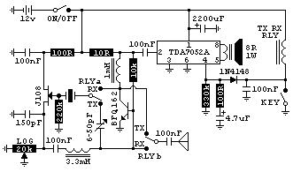
minimum resistance that allows reliable oscillation) as measured at the FFT is 925mW at 50 ohms at 40m amd the higher bands, with a supply of 12v. At 80 and 160m, the output power drops a bit to around 700mW, but I only had one crystal in each band to test this. Note that if ultimate harmonics performance is your goal, then an LPF could be used at the output of the transceiver, for the bands of interest. However, at these QRPp powers an LPF is not always needed, as harmonics interference will be minimal anyway. You may even want to build a BPF instead, which will be a benefit to the receiver, to knock out interference by strong commercial broadcast stations. Note that the transceiver is a broadband circuit, it can be used to transceive even outside the HAM bands. Just hook up an HF crystal and you are redy to go. This feature might be useful if you want to receive a commercial transmitter outside the HAM bands, but do not use it to transmit, as this will not be legal. The offset mechanism has also been changed in this version. I replaced the switch and the fixed capacitor with a single 6-50pF variable trimmer capacitor. This reduces the transceiver to one component less and it allows to set the TX offset at any value you like. At 1.8MHz the maximum TX offset is about 500Hz with this capacitor set to minimum so this seems to be better than the single 8.2pF capacitor I used before. 50pF seems to be ok for adequate offset at 28MHz. On 160m and 80m just set this capacitor to minimum and on the higher HF bands on maximum. The TX is on USB, meaning that the TX carrier is shifted above the RX carrier durring transmission. The final change was to reduce the value of the regeneration potentiometer to only 10k. Single signal reception is now not possible at lower bands because the oscillator signal cannot be set to zero. However this change allowed a much more smoother adjustment of the regeneration (and hence the output level) at the higher bands, which was a must. Practically, single signal reception really reduces the sensitivity of the receiver and requires more AF gain that is available by the single AF stage. In favor of the sensitivity and the smooth regenration adjustment at higher bands, the single signal reception option was removed. |
|
|
|
  |
Ultra
minimalism calls for high impedance phones or a PC to be connected to
the transceiver. But such phones may not always be available and in
some cases very hard to find. A PC may not always be the case,
especially in portable operations. Also, the need for an extra set of
cables from the transceiver to your ears, could make things messy, in
portable operations. You might feel perfectly ok with high impedance
phones and that is absolutely fine. However whenever speaker volume is
needed an extra audio amplifier needs to be connected to the
transceiver. There are different options but for minimum components count the IC solution seems the most favourable by many (well, if an IC can be considered as one component). You may think that this is not a discrete transceiver any more and you are right. But from the simplicity point of view, there is no beat to it. The classic way is to go for the LM386, but I do not like this because it adds quite a lot of components, like a discrete AF amplifier would do. The TDA7052A seems to be the simplest amplifier to use. With just three more components added to the transceiver, you have speaker volume and volume control option (with the 470k potentiometer). These are advantages that can't be easily ignored just for the shake of using an IC instead of going discrete. Note that the TDA7052A that I use, has a different volume control mechanism than that of the TDA7052 (without the "A"), and because of this, only one AF coupling capacitor is required. The amplifier works perfectly, providing quite a lot of audio volume to the speaker, for comfortable listenning. When the transceiver is in TX mode, noise is heard from the speaker because the AF amplifier power is not disconnected during that time. The noise level depends on the setting of the regeneration potentiometer (the TX output power). Also when the TX/RX switch changes state, loud clicks are heard from the speaker as it is expected. |
|
|
|
  |
In
this version I have done several changes. I have removed the PC keyer
circuit to make the schematic look less messy. If you still want to
build this, look at the previous versions. However I have kept the
relay to switch between the TX and RX. One reason is that I could now
use a SPST switch to key the circuit. This also allows an external key
to be connected to the circuit, which is preffered by many HAMs. I
thought relays were quite expensive, but a search at the internet
revealed prices as low as 0.3 Euros for small DPDT 12V relays. I used
the smallest I could find to minimize noise from the relay contacts.
The other reason I used the relay, was that I could use the SPST switch to also mute the AF amplifier during TX and during TX/RX switching, which otherwise produced lots of AF noise. The 4.7uF and the 100R in series, provide the correct timing to un-mute the AF amplifier on key-up. The 100nF parallel to the key helps on this too. I have also removed the AF volume potentiometer as the volume at maximum position is neither too low nor too high. I would say it is medium to high, but it is convenient to listen and there is no real reason in going quieter. I also lowered down the gain of the chip using a 330K, to avoid the weird noises the chip produced at high gains. I have also changed the BJT collector choke to 1mH. The 3.3mH molded choke was getting very hot so a more powerful choke was needed. This choke had to be suitable for HF. The Amidon FT50-77 toroidal core can be used to build chokes for 1-50MHz and it offers very high AL. The wire to be wound onto it must be of big diameter so as not to get hot. So the BJT 1mH choke is built with 30 turns of 0.54mm diameter enameled wire. You will need no more than 50cm of wire. This will give an inductance of 1mH, which is lower than the previous 3.3mH but works flaulessly. The purpose of the choke is to allow DC and audio to pass through but block the HF RF power from flowing through it, so 1mH is fine. The last change was to replace the regeneration potentiometer with a 20K logarithmic. This allows the output power to be set at lower levels at around 40m where the gain of the oscillator is more and at the same time it does not affect the smooth setting of the regeneration (and the output power) at higher bands, due to the logarithmic curve. The way you should connect this potentiometer is as follows. As you see it in the schematic, set the potentiometer wiper at the middle point. Then measure the resistance from the middle pin to the left and right pins of the pot. The resistance at the right side should be lower than that of the left. This is the correct way, not the other way round. You could also try to find a regeneration potentiometer with a switch embedded to it. If you can find one, then you do not have to have an extra ON/OFF switch. |
|
|
|
 |
This
is an experimental untested version, where I was trying to make an
output filter for the transceiver. Do not build this one yet as I have
not tested it. |
|
|
|
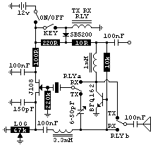   |
In
this version there are two major improvements to the circuit. First,
the power consumption on RX has been minimized to about 35mA at 12v.
Second, the audio output volume has been greatly improved. Now this can
be really considered a battery friendly transceiver as well as a
transceiver that is able to drive comfortably a set of high impedance
earphones, without further audio amplification. The trick for both of these improvements, is to make the collector resistor larger during RX and smaller during TX. This is accomplished by a different key arrangement and an additional resistor and diode. During RX the BJT collector is connected to the 10R and 220R in series, forming a total collector resistance of 230R. During TX the key shorts the 220R through the diode and the collector resistor is now only the 10R. The relay is now necessary in this configuration and a simple DPDT switch cannot be used anymore. The 220R could be made much larger if you wish and this has an effect in the RX current, with no difference in the audio output volume. Just for reference, with 1K instead of 220R, the current on RX was 10mA and with 10K, just 1mA. The only reason a 220R was placed there, was because I started to notice weird AF oscillations in some regeneration settings, as this resistor was getting larger. The diode is a power schottky for low voltage dropout. Use any type you have on hand, it is not critical, as long as it is a power schottky. |
|
|
|
 |
In
this version I have replaced the dual relay with a quad type. If you
don't have a quad relay, you can use two dual relays instead. If they
are 6v, connect their coils in series. If they are 12v, connect their
coils in parallel. The use of another set of relay switches has three
significant advantages. First, the key can be grounded again. The key can also be used now for audio mute on TX. This is an important feature and without it you can easily get deaf by the loud audio clicks in your ears during TX and RX switching. Second, one relay contact can be used for short circuit the 220R resistor without the need for a diode. This avoids having to find a power schottky but also avoids any voltage drop that would be caused by the diode. The third and the most important advantage, is that one relay contact can be used for individually set the TX and the RX regeneration. This was an issue I had from the early stages of the design of this transceiver. The source potentiometer setting on RX, was not optimal for TX and vice versa. When the setting was done on RX for optimum RX performance (higher audio output volume or LSB rejection), this setting was causing the TX to operate at much lower output power than possible with this transmitter. On the other hand, if the TX was set for maximum output power, this setting made the RX too insensitive to incoming signals. Both of these disadvantages are solved by the extra relay contact and an extra potentiometer. Now, one potentiometer is used for correct regeneration settings on RX and another one is used for setting the output power on TX. The relay contact switches back and forth on these two potentiometers. With this solution you also add the TX power setting feature, which is useful in case you only want to make local contacts, or if you want to drive an external power amplifier with the correct input signal level. |
|
|
|
 |
In
the previous version the audio mute feature did not work, as I was
dumping audio through the relay coil. In this version a diode isolates
the relay circuit and the key from the audio and at the same time
provides the desirable mute function. Since now there is no DC in the phones, the extra 100nF capacitor is not needed anymore. I have also increased the 100nF audio capacitor to 10uF. The reactance of the 100nF at 700Hz is over 2Kohms, which means that with 1Kohm phones some audio volume would be lost. |
To be continued...