Diode
amplifier
Conceived and designed
by sv3ora
26-Feb-2021
My previous experiment with the Saturable Inductor Amplifier,
gave me another idea. Why not use a diode in place of the inductor and
shunt RF to ground using this diode? Thus, my Diode Amplifier was born.
My Diode Amplifier, is based on the
principle of diodes used as switches. In this page, I am going to perform a
number of practical experiments, to show how my Diode
Amplifier can be used to perform different functions in electronics. In this page, I am going to experiment with it in
different circuits.
Inverter logic gate
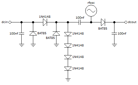
The easiest way to explain the operation of my Diode
Amplifier, is by looking at the circuit diagram above. The diagram
shows an inverter gate I have built and tested, which works in the
following way. When "dcin" is disconnected or tied to ground (logic 0),
the "rfosc" RF signal passes through the right diode, it is rectified
and it charges the output shunt capacitor, to create a voltage on
"dcout" (logic 1). At the same time, the RF signal passes to the left
side through the middle capacitor and the negative portion of the
signal, is clipped to groung from the middle reverse diode and the
reverse diode at the input of the gate. The positive portion of the RF
signal cannot
escape through the left series diode. The only way this positive
portion can escape to the ground, is through the lots of series diodes
to the ground. To avoid clipping of the usable positive RF signal, we
put more series diodes. So, a logic 0 at the
input of the inverter gate, results in a logic 1 at it's output.
If DC is applied to the "dcin" (logic 1), it is filtered from any RF by
the left capacitor and it passes through the series diode, to the
middle shunt diodes, where it drives the lots of series diodes into
conduction, opening a path for the positive RF signal out of the "rfosc" to flow to the ground. With most RF signal flowing to the ground, there is little or
any signal left to pass to the right voltage rectifier.
The right capacitor is then discharged through the load connected to
the "dcout" and reaches logic 0. Hence
a logic 1 at the input of the inverter gate, results in a logic 0 at
it's output.
Comparing my Diode Amplifier to my
Saturable Inductor Amplifier, in the Saturable Inductor Amplifier there
is no such thing as clipping, but in the diode Amplifier,
we have to put more series diodes to avoid clipping. I do not know if
this is a disadvantage or not, as one can set the gate gain by
adjusting the number of series diodes accordingly. The good thing about
this Diode Amplifier is that it can operate even at very low AC
frequencies (even mains AC!) in contrast to my Saturable Reactor
Amplifier, so this can be made purely with passive circuicity including
the AC signal.
To be continued, be patient please...
Back to main
site