
by SV3ORA
Fine tuning the SM0VPO HF
amplifier for better performance
by SV3ORA
This is a modification of the popular SM0VPO broadband HF amplifier, for better performance. The schematic of the amplifier and the winding of the transformers is described in the original article presented at the end of this page.
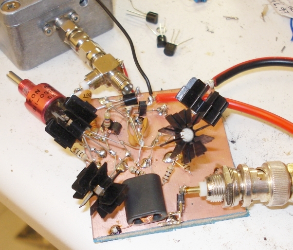
The first modification that has to be done, is to use known transformers, in comparison to the ones SM0VPO has used that were unknown. This ensures that anyone can rebuild this amplifier with similar performance.
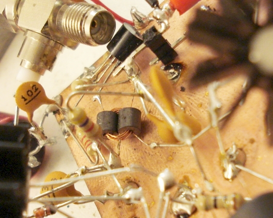
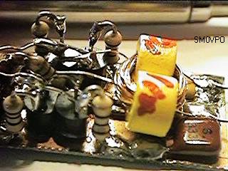
For the first phase splitting transformer, I used a pair of FB-43-101 ferrite beads, put together like shown in the picture above, to form a single transformer core.
For the second power transformer, I used a BN-43-202 ferrite core, like shown in the picture above.
The next modification, had to do with the transistors that were used. I have to say, SM0VPO was a little optimistic in that sense. With the BC547C transistors in the final amplifier section, the continuous power output was about 350mW maximum! The transistors were getting quite hot if driven harder. The peak power that I could get was about 500mW and this was ok for only 1 or 2 seconds. Then the signal started to get very distorted, as the transistors were getting hot.
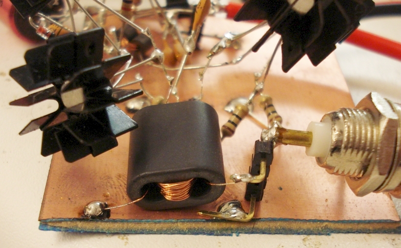
I knew that I could get more power out if this little amplifier. The modification that I did, was to use the 2N2222A metal transistors at the final amplifier section, instead of the BC547C. This allowed the attaching of small heat sinks onto them, to raise the dissipation and at the same time to make the amplifier withstand more SWR. I used a simple multi meter transistor matcher, to match the transistors for HfE, as I thought this would be a good idea.
With these heat sinked transistors used, I have managed to take a continuous output power of around 700mW, without distorting the output waveform at all. I managed to drive the amplifier harder, by applying more input signal and raising the voltage a bit from 12v to 13.8 and 15v. Then the amplifier outputs 1W, without significant waveform distortion. After this point, the amplifier starts to clip.
The improvement was obvious. Still using inexpensive transistors, I could get a 0.7W-1W output from this little monster, with a current consumption of 150-200mA depending on the voltage and input signal. Now, compare it with the 0.3W-0.5W of the original amplifier.
I have also tried to change the driver transistor to a 2N2222A and BC109C. The gain was worst than the BC547C in this place, so I left this transistor to be a BC547C, as in the original circuit.
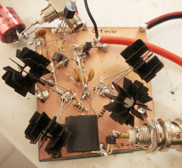
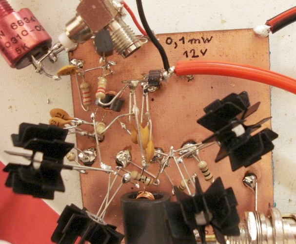
With my modifications on this amplifier, the signal at the input of the amplifier was 0.1mW for an output of 700mW at 12v. That is -10dBm compared to the original circuit, which had only -4dBm. SM0VPO's version has a total gain of 30dB whereas my version has a measured gain of 38dB to 40dB.
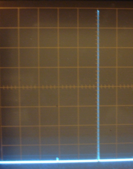
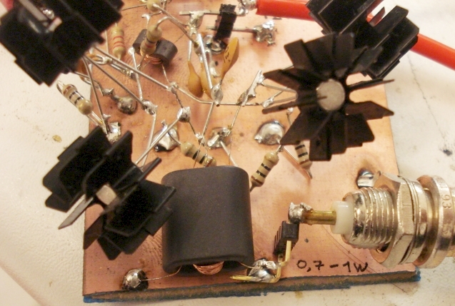
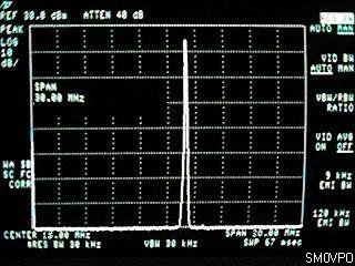
All the measurements, were performed on the single frequency of 10.7MHz. My oscillator had an output of about +9dbm, so I connected a 5K potentiometer at it's output as a voltage divider, to be able to set the desired output power. At this stage, I did not care too much about impedance matching. Picture above, shows the main 10.7MHz signal on the right and the second harmonic on the left. I did not perform accurate measurements but with a rough view, it seems the harmonic is more than 25db down, but this is very rough.
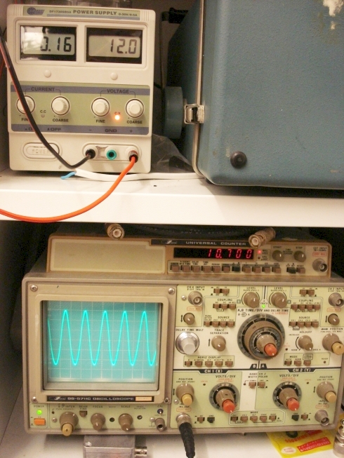
Picture above, shows the voltage and current drawn, as well as the output signal waveform at about 0.7W at 50 ohms. Not too bad for such a simple amplifier.
Original article from SM0VPO below
This project was a particular surprise for me in that the BC547 (equiv 2N2222) can be used to build a 500mW linear amplifier covering the entire HF band with excellent spectral purity and no neutralizing at all. Ugly-bug construction was used but I dare say that the good results are partly to do with the method of construction.
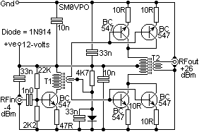
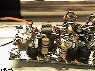
The circuit is fairly straight-forward and does not even need any form of RF neutralizing. Two pairs of BC547 transistors are used in a push-pull type of output stage, biased by a single diode and resistor. The driver is also very conventional using T1 to transform the drive impedance to a very low value for the output pairs. The amplifier is constructed on a piece of copper-clad board 45mm long by 17mm wide. Superglue a 44mm long by 3mm wide strip of copper-clad board along the center. This will become the battery supply rail. Using a sharp knife, remove some copper to form a 3mm x 3mm pad at one end of the battery rail to form the RF output terminal. Next fit the 10n and 33n decoupling capacitors; one pair at either end. These should lay flat on the board. The rest is easy after you see the photographs.
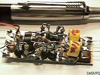
T1 primary is 14-turns of very thin wire (0.1mm Dia.) and the secondary is 1+1 turn of thin wire (0.2mm Dia.). T1 former is two of the smallest ferrite beads I could find. You can just see it in the left-hand photograph above. T1 is composed of two grey ferrite beads. The right-hand photograph shows T2 and the mounting of the two output pairs of BC547 transistors.
T2 is a little special. I found two small ferrite rings in the junk-box and decided to give them a try. The windings are 11-turns triflar wound using thin wire (0.2mm Dia.):
The five transistors are all mounted on their heads using super-glue and with their legs in the air spread wide apart (Hey! this sounds kinda' pornographic!!). The finished linear amplifier does not look very pretty but it is very small. It is less than 10mm high and looks like this. Here you can see it beside my parker pen for comparison (I thought it would be better than a common 1-crown coin).
Spectral purity was the biggest surprise; nothing to see on the analyzer! Not a single unwanted blip, peak or spurious signal over -30dBm which is about 60dB down on the fundamental. Not bad for "ugly-bug" construction. The amplifier has a 30dB gain so the full output can be achieved when driven from a normal signal generator. Note that Heterodyne generators, such as the Marconi TF995, usually have a very dirty output signal and are not suitable as a driver as the basis of a transmitter; just because it cost you money does not mean it is perfect (as any ham's neighbor owning an Onkyo color TV will testify). The bandwidth extends well into the VHF region but the gain is almost unity at 100MHz. Here is the spectrum analyzer displays. The left-hand photograph shows a sweep of the band from 0-30MHz centered on 15MHz. The input is 17MHz. The right-hand photograph shows the frequency response, scale is also 3MHz/division and the top line is +30dBm (1-watt) on both traces. The scales are logarithmic with 10dB per division.
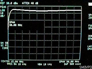
The input level is -4dBm (400uW). As you can see, the gain is reasonably flat and quite useful from less than 1MHz to well over 30MHz. Ok, so now you have all the information you need to build the linear amplifier yourself. Now that you have got it, what can you do with it? You may want to try:
Please do not ask me silly questions, such as what was the relative humidity and barometric pressure when I wound the transformers or even the density of the ferrite cores I used. I haven't got a clue. It is as you see it, a rather slack-handful of resistors and the rest from the junk-box. If you use a different type of ferrite then the bandwidth may change a little, maybe not covering medium-wave (add more turns to T1 and T2) or perhaps a lower output in the 35MHz radio-control band (remove a few turns from T1 and T2).