Saturable
Inductor amplifier
Conceived and designed
by sv3ora
22-Feb-2021
Magnetic amplifiers and logic, always fascinated me. Magnetic
amplifiers were used for a large period in time (and still do in some
applications). However, magnetic logic seems to had appeared for a
short period of time, in an era where there was switching from vacuum
tubes to transistors. There were some circuits and devices developed
and in one case a full computer has been built out of magnetic logic.
There are also documents on the net about magnetic logic that uses no
diodes at all to perform the function. However, most of the documents I
have found, do not give enough information of how to build practical
devices out of magnetic circuits, as they do not contain all the
details needed for a successful implementation. I believe that apart
from experiments and demonstration devices, magnetic logic was never
really given the chance to prove it's capabilities, due to the new
coming transistor technology which dominated everything.
I have performed a number of experiments in the past, implementing my ideas or existing ones, using all shorts of magnetic things, like square loop toroids, pulse logic and core rope memories. This time, my RF background made me re-think of the whole thing and eventually I concieved a new device, which I call Saturable Inductor Amplifier
(in contrast to the saturable reactor amplifier). This "device of
amplification" can be used to built magnetic amplifiers and magnetic
logic devices, posing significant advantages over the magnetic logic
devices that were developed in the past:
- Cheap, easy and practical to implement, even from unskilled experimenters and even on larger scale circuits.
- No special magnetization cores (square loop) are needed.
- No special shape cores (multi-aperature, H-cores etc.) are needed.
- No difficult winding techniques are needed (in fact no wiring at all is needed, as standard commercial parts can be used)
In this page, I am going to perform a
number of practical experiments, to show how my Saturable Inductor
Amplifier can be used to perform different functions in electronics.
First of all, I am going to begin with a simplistic explanation of the
basic principles of operation and afterwards experimenting with it in
different circuits.
My Saturable Inductor Amplifier, is based on the combination of the
principles of inductor core saturation and RF blocking (choke action).
I was introduced in the core saturation principle by reading books
about saturable reactors, and in RF blocking mostly experimentally,
through the large number of HF radio experiments I have performed
throughout the years. Essentially, with this device, I combined
magnetism with radio.
Inverter logic gate
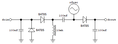
The easiest way to explain the operation of my Saturable Inductor
Amplifier, is by looking at the circuit diagram above. The diagram
shows an inverter gate I have built and tested, which works in the
following way. When "dcin" is disconnected or tied to ground (logic 0),
the "rfosc" RF signal passes through the right diode, it is rectified
and it charges the right shunt capacitor, to create a voltage on
"dcout" (logic 1). The RF signal from the oscillator, passes also to
the middle capacitor and reaches the middle diode
and the choke inductor. The positive portion this alternating RF signal, cannot
escape through this diode, but it is also
prevented from reaching the ground,
due to the high inductance value of the choke. I say the positive portion
of the alternating RF signal, because the middle capacitor causes the
RF signal to go below ground at half of the cycle and so, there
is also a negative portion that can pass through the middle diode. This
negative portion is sent to ground through the left diode, so as not to leak to the dcin port. So, a logic 0 at the
input of the inverter gate, results in a logic 1 at it's output.
If DC is applied to the "dcin" (logic 1), it is filtered from any RF by
the left capacitor and it passes through the middle diode, to the
choke and the middle capacitor. The middle capacitor blocks any DC from
flowing further, so DC can only reach the ground through the choke
inductor. As DC passes through this inductor, it saturates the inductor
core, dramatically decreasing it's inductance. This decrease in
inductance opens the way for the RF signal out of the "rfosc" to pass
through the middle capacitor and the (now saturated) choke to the
ground. With most RF signal flowing to the ground, there is little or
any signal left to pass through the right diode and the right capacitor.
The right capacitor is then discharged through the load connected to
the "dcout" and reaches logic 0. Hence a logic 1 at the input of the inverter gate, results in a logic 0 at it's output.
For the circuit to work efficiently, the inductor must be as small in
physical size as possible (small core), but at the same time to have a
large number of turns. Thus, core materials such as the 75 (J) ferrite,
are possibly not suitable, because they require a few turns to reach to
high inductance values. This means that they require more current (and
thicker enamel wire) to saturate at this low-turns number, which would
make the gate inefficient. A good starting point, seems to be these
standard 10mH 1W molded chokes that are sold in quantities for very low
prices. If you use such or similar inductors, you won't have to wind
anything yourself. A good thing about the circuit is that it can be
scaled up into larger powers easily, by feeding it with a higher
current/voltage RF source. The output diode-capacitor can handle lots
of power if appropriate power components are used.
To be continued, be patient please...
Back to main
site