COLLECTED BY
Organization:
Internet Archive
The Internet Archive discovers and captures web pages through many different web crawls.
At any given time several distinct crawls are running, some for months, and some every day or longer.
View the web archive through the
Wayback Machine.
Web wide crawl number 16
The seed list for
Wide00016 was made from the join of the top 1 million domains from CISCO
and the top 1 million domains from Alexa.
TIMESTAMPS
Experiment about the Gilbert cell double balanced mixer.
It may be the spell miss of the Gilbert cell double balanced mixer. I know
the name only in Japanese. I have used this type of circuit as the IC.
TA7320 and TA7310 are the Gilbert cell double balanced mixer made by Toshiba
company. It is famous as MC1496 or SN76514 in U,S,A. I used them as a black
box for many years. But in these days my inter net friend taught me that
this circuit is based on the differential amplifier. I made some experiment
about this circuit. And I feel that I could understand how it works.
gil2.gif
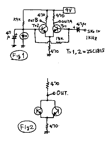
See the figure 1! This is the differential amplifier. The transistor1 works
as a emitter grounded amplifier. Therefore on the OUTA port ,there comes
the inverted phase signal of the input. The transistor2 works as a base
grounded amplifier. Therefore on the OUTB port ,there comes the non inverted
phase signal of the input. When I input the 40mVc-p (Center to Peak) 1kHz
signal on the SIG IN port , both amplitude of the output ports were 300mVc-p.
Therefore when I connected the OUTA port with OUTB like the figure2, very
small signal (10mVc-p) became on the OUT port. The inverted signal of the
OUTA might have canceled the non inverted signal on the OUTB port. This
type of mixer was used on the ancient tube receiver with 12AU7 named tube.
gil3.gif
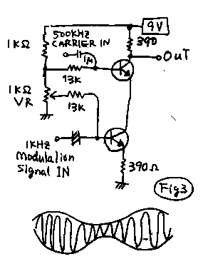
As a next experiment , I made tohempole mixer. See the figure3! With inputting
the modulation signal on the downside transistor, the carrier signal of
the upper side transistor was modulated by the modulation signal. I can
watched the amplitude modulated signal on the OUT port on the cathode ray
tube of my oscilloscope. I had to tune the bias control potentio meter
"variable resister" to get such a beautiful signal. On the Gilbert
cell , basic theory of it*s modulator based on this figure. Lower side
transistor modulates the upper side transistor. But on the Gilbert cell,
the carrier signal itself do not came on the output port. Also, the modulation
signal itself do not came on the output port. Both basic signals were canceled
by the circuit. I will explain how it works, how the Gilbert cell cancels
the carrier signal and modulation signal.
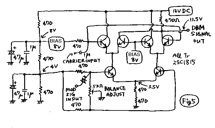
gil4gif
See figure 4! Three differential amplifiers are connected. I named all
the transistors and resisters as this figure. Connect IN1 and IN2! I named
it as LOIN " Local oscillator input". Connect OUT12 with OUT21
port! I named it as OUTf " out final". The modulation signal
put on the IN3 port produces inverted current on RL31 resister. This current
is divided for Q11 and Q12. And this current flows on the RL12 resistor.
On the other hand, the modulation signal put on the IN3 port produces "non"
inverted current on RL32 resister. This current is divided for Q21 and
Q22. And this current flows on the RL21 resistor. Therefore , the modulation
signal do not came out on the OUTf port , as the result of canceling of
the two currents. The carrier signal input on IN1 port produces non inverted
signal on the OUT12 port, because Q12 works as the differential amplifier.
The carrier signal input on IN2 port produces inverted signal on the OUT21
port, because Q21 works as the emitter grounded amplifier. Therefore ,
the carrier signal do not came out on the OUTf port , as the result of
canceling of the two currents. In order to complete this circuit, please
short the useless resisters! The name of the useless resisters are R11,R22,
RE1,RE2,RL31,RL32. You can understand this circuit is the famous Gilbert
cell. Rechte gemacht!
gil5.gif
I felt that I could understand the Gilbert cell. In order to complete this
experiment, I made this circuit on the discrete board. All the transistors
are 2SC1815-Y. I do not know they may be the same lot. But I bought them
on the same package "1500 yens with 200 pieces". I did not feel
so happy when I turn on the power switch. Because it produced the beautiful
doubly balanced signal in instantly, as it indicated " you can see"
on the picture. But I felt a small happiness when I tuned the balance adjust
resister. The carrier null point was different from the modulation signal
null point.
gilph.gif
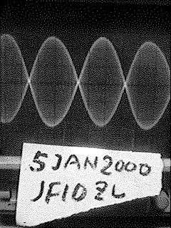
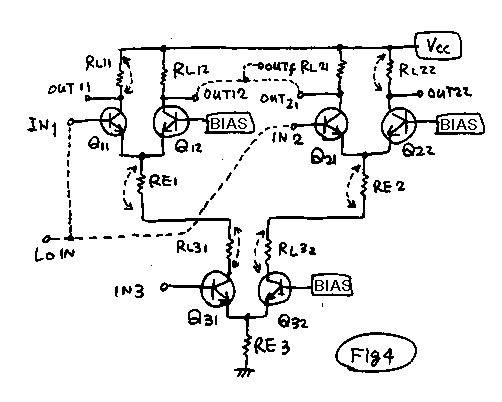
The performance of the circuit indicated on the figure 5.
The Carrier was 7-mVc-p 500kHz.
Modulation signal
(mc-p) |
Output signal
(mVc-p) |
Gain(dB) |
Carrier suppression
(dB) |
| 0 |
10 |
- |
0 |
| 10 |
70 |
16.9 |
-17 |
| 20 |
170 |
18.5 |
-25 |
| 30 |
220 |
17.3 |
-27 |
| 38 |
270 |
17.0 |
-29 |
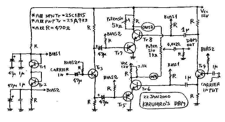
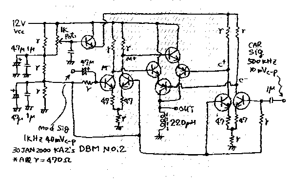
Kazuhiro*s cell -----add description on 23 Jan 2000
I tried to make a new circuit to act as a double balanced mixer like a
Dilbert cell. My American friend taught me that the name what I say may
be "Dilbert". But I already named this page as "gil. Html".
To change the name of the page is very difficult for me HIHI.****Description
add on 2 May2001***Japanese electric magazine named for " Transistor
technology" on May 2001 introduced us the developer of this circuit
as Mr.Barrie Gilgert with his photo. He is a Manager in Analogue devices
Co. ******
1. As a first basic part of double balanced mixer , I made a phase inverter
of the modulating signal. For this purpose, Dilbert uses a differential
amplifier. I use an collector emitter divider , like a plate cathode divider
of the Williamson amplifier. See fig7! The transistor named Tr3 works for
this purpose.
2. As a second basic part of double balanced mixer , I made a phase inverter
of a carrier signal. Dilbert uses a differential amplifier also for this
purpose. I use an collector emitter divider also for this purpose. See
fig7! The transistor named Tr4 works for this purpose.
3. As a third basic part of double balanced mixer , I made a mixer. For
this purpose, Dilbert uses a NPN NPN totem pole. I use an emitter connected
NPN PNP totem pole for this purpose. See fig7! The transistor named Tr5
and 6 work for this purpose. This part makes an amplitude modulated high
frequency signal.
4. As a fourth basic part of double balanced mixer, the same type mixer
must be made as a last one. But for this mixer, the inverted modulating
signal and the inverted carrier signal must be used. Frankly to say, I
did not want to use the capacitor for connecting this mixer with the twin
divider. I wanted to connect them directly. But I cannot develop any bias
system to joint them directly.
5. As the end of the double balanced mixer, twin amplitude modulated signals
must be combined. See fig7! The potensio meter 1k ohm works for this purpose.
This part makes an double side band signal from a pair of AM signals. The
potensio meter must be tuned to make minimize a leak of the carrier signal
500kHz on the OUT port. You can see the 0.0022 micro farads capacitor and
R= 470 ohms resistor near the OUT port. It is a high pass filter to reject
a modulating signal on the OUT port.
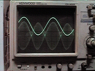
You can see the photo 2. The carrier suppression is not so good as the
Dilbert's cell. I will write the total performance on the same time as
I got this photograph.
Modulating signal: 1kHz, 30mVc-p
Carrier signal: 500kHz, 7mVc-p
Output signal: 30mVc-p
Carrier leak : 6mVc-p
Carrier suppression: -13dB
You may be able to construct some kind of double balanced mixer circuit.
You will be able to use a dual gated FET on the mixer. You will be able
to use a wide band transformer made with ferrite beads for the phase inverter.
The total performance will be great or poor, depending on which type of
circuit do you choose. Isn't it joyful to think about such a new circuit?
gil7.gif
gilph2.gif : Uppersign wave is a modulating signal 1kHz. The lower signal
is DSB signal.
gil8.gif
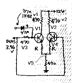
30Jan2000***discription add about the experiment of differential amplifier
and the modification of Kaz's double balanced mixer
1. the experiment of differential amplifier
I learned on the Motorola data book about MC1496 that the gain of the Dilbert
cell can be changed by the external resister of the emitter. And I thaught
that this resister may be able to adjust the current balance of the differential
amplifier. See fig8! I put the two resisters on the emitter of the differential
amplifier. I learned how these resistors works. See the data table.
***V1=voltage of the collector of left transistor.
***V2=voltage of the collector of right transistor.
***V3=voltage of the common resister.
***V4=voltage of the emitter of left transistor.
***V5=voltage of the emitter of right transistor.
***dV=V1-V1 (difference of collector voltage)
***n=dV/(Vcc-V1)*100% (difference percentage of collector voltage) ***vin=50mVc-p
constant modulating signal 1kHz
***v1=signal of the collector of left transistor.
***v2=signal of the collector of right transistor.
***dv=v1-v2(difference of collector signals)
***z=dv/v1*100%(difference percentage of collector signals)
***g=20log(v1/vin) (voltage gain of signal)
***rezult1:To improve the difference percentage of collector signals, R
must be about10% of the emitter common resister.
***result2: To improve the difference percentage of collector voltage,
R is the the bigger the better.
***result3: To get more gain , R is the smaller the better.
| R |
ohm |
0 |
4.7 |
22 |
47 |
210 |
| V1 |
DC volts |
10.80 |
10.63 |
10.53 |
10.54 |
10.67 |
| V2 |
DC volts |
9.97 |
10.15 |
10.29 |
10.37 |
10.64 |
| V3 |
DC volts |
3.37 |
3.26 |
3.20 |
3.13 |
2.69 |
| V4 |
DC volts |
3.37 |
3.27 |
3.26 |
3.27 |
3.25 |
| V5 |
DC volts |
3.37 |
3.37 |
3.32 |
3.28 |
3.26 |
| dV |
DC volts |
0.83 |
0.48 |
0.24 |
0.17 |
0.03 |
| n |
% |
69 |
35.0 |
16.3 |
11.6 |
2.25 |
| vin |
mVc-p |
50 |
50 |
50 |
50 |
50 |
| v1 |
mVc-p |
1.0 |
720 |
350 |
190 |
60 |
| v2 |
mVc-p |
1.1 |
750 |
350 |
190 |
45 |
| dv |
mVc-p |
0.1 |
30 |
0 |
0 |
15 |
| z |
% |
10 |
4.1 |
0 |
0 |
25 |
| g |
dB |
26 |
23.2 |
16.9 |
11.6 |
1.5 |
gil9.gif
2. the modification of Kaz's double balanced mixer By using modified differential
amplifier, I made the modified double balanced mixer. See the fig9! I show
you the total performance of it.
Modulating signal: 1kHz, 40mVc-p
Carrier signal: 500kHz, 10mVc-p
Output signal: 2000mVc-p
Carrier leak : 120mVc-p
Carrier suppression: -24dB
gil10.gif
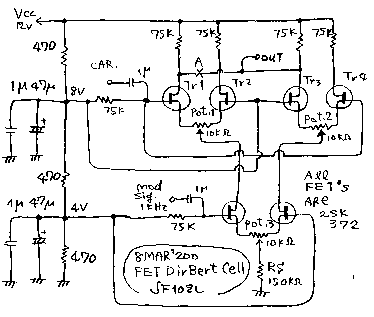
8Mar2000***discription add about the experiment of differential amplifier
."Double balanced mixer made with FET"
See the upper circuit! I have already enjoyed to make experiment about
DBM for this three month. I wrote 3 notebooks about it. I will show you
the double balanced mixer made with FET*s.
The performance of it is as follows.
Carrier signal: 100kHz, 400mVp-p
Output signal: 550mVp-p
Carrier leak : non ,but double frequency of carrier signal leaks 50mVp-p
How to tune this circuit
1.Cut A point !
2.Omit the carrier! Input only the modulating signal! Tune pot 1 to balance
the signal of drain of Tr1 and Tr2!
3. Tune pot 2 to balance the signal of drain of Tr3 and Tr4!
4. Tune pot 3 to balance the signal of drain of Tr1 and Tr3!
5. Connect A point! And input the carrier!
Comment
1. To make a good differential amplifier with FET, The higher gm the better.
The FET 2SK372 has 60mS as it*s gm.
2. To make a good differential amplifier with FET, The higher the soace
resister the better.
3. I did not get the pare tubes for this gear, I must make balance one
by one.
gil11.gif*****fig11.
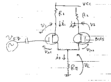
Description add on 30 Mar 2000***** Calculation of signal balance of differential
amplifier made by FET.
In order to make a good carrier suppression with the Dirbert cell, I must
make good balanced differential amplifier with FET. In order to make good
differential amplifier, I must use big gm FET. And also I must use big
resister for the source. I learned them from experiment. But I did not
understand the reason. I made calculation about the signal balance of differential
amplifier to understand the reason. See fig11!
v1: the signal out on the drain of left FET
i1:signal current on the drain of left FET
vin1: the signal input of left FET= voltage between the gate and source
gm1:Conductance of left FET
i1=gm1*vin1....................(1)
v2: the signal out on the drain of right FET
i2:signal current on the drain of right FET
vin2: the signal input of right FET= voltage between the gate and source
gm2:Conductance of right FET
i2=gm2*vin2....................(2)
i3=i1+i2................................(3)
ve: voltage of source is decided by the current flows on Re resister
ve=i3*Re..............................(4)
vsig: signal voltage on the gate of the right side are sum up of ve and
vin1
vsig=ve+vin1........................(5)
The gate of the right side FET is fixed by bias voltage.
vbias=ve+vin2=0..................(6)
v1: signal voltage of the drain of the left FET is culculated by the current
of drain resistor.
v1=-R1*i1.............................(7)
About the right FET, the same way.
V2=-R2*i2...............................(8)
All the actors are on the stage now.
(1) ,(2).....to (3)
i3=vin*gm1+vin2*gm2..........(9)
(9) ......to (4)
ve=( vin*gm1+vin2*gm2)*Re.....(10)
from (6)
ve=-vin2...............................(11)
(11) ....to (5)
vin1-vin2=vsig.....................(12)
(11) .....to(10)
-vin2=(vin1*gm1+vin2*gm2)*Re.......(13)
from (12)
vin1=vsig+vin2...................(14)
(14) ....to(13)
-vin2=( (vsig+vin2)*gm1+vin2*gm2)*Re
-vin2=vsig*gm1*R1+vin2*gm1Re+vin2*gm2*Re
-(1+gm1*Re+gm2*Re)*vin2=vsig*gm1*Re
Therefore
vin2=-vsig*gm1*Re/(1+gm1*Re+gm2+Re)....(15)
(15) ....to(14)
vin1=(1+gm2Re)/(1+gm1*Re+gm2*Re)........(16)
From (7),(8)
v2/v1=R2*i2/R1*i1................(17)
(1) ,(2)....to(17)
v2/v1=R2*vin2*gm2/R1*vin1*gm1.............(18)
(15) ,(16)....to(18)
v2/v1=-R2*gm2*Re/R1*(1+gm2*Re)...........(19)
What I say from the (19)....1
If "gm*Re" is big enough than 1 , v1 and v2 become the same signal
width. But in actual FET , gm = 10m mho, Re= 100 ohm. Therefore gm*Re=1.
What I say from the (19)....2
Anyway v2 must be smaller than v1.
What I say from the (19)....3
To get big "gm*Re" , we must use big bias voltage , and to use
the FET with bigger Re resister.
ギルバートセル型ダブルバランスドミクサー(以下DBM)の試作と実験(5JAN’00)
私が、初めてアマチュア無線家として、いわゆる電話の交信に成功したのは、別のページで紹介してある「21MHzDSB送信機」でした。この送信機には、
TA7320PというIC式のDBMを使っていました。その製作にあたっては、7000円で買った東芝のICのデータブックの中に、TA7320Pの等価
回路が描いてありましたが、当時の私にはその回路がなんの事やらさっぱり分かりませんでした。それでもそのまま、雑誌の回路例と同じ様に組んだ所、同じ様
な波形がオシロで観察できるDSB信号がえられたので、そのままずっとこのICを使ってきました。最近、JA−QRPクラブのメールのやり取りの中でこの
回路(ギルバートセルというそうです。)の動作が話題となり、これが作動増幅器を基本にした回路である事がわかりましたので、それが「引き金」となって、
いくらかの実験を行い、この回路の事が私なりにわかりました。以下に私の行った実験と、考察を紹介して、この回路の解説をしてみます。ちょっとややこしい
話になりますが、頭の体操だと思って読んでください。
gil2.gif
まず、図1の回路を組んでみました。これが差動増幅器の基本回路です。トランジスター1は、エミッター接地として動作しています。ベースから入力された、
低周波信号(ここでは、自作のウイーンブリッジ発振器で作った1kHz40mVcーpの低周波信号を使って実験した。)は、Tr1のコレクターに
300mVc−pの信号として現れます。一方、Tr1は同時にエミッターフォロワーとしても動作しており、エミッターにも入力信号と同じ大きさの信号が、
0.5ボルトの減算された形で現れます。一方、Tr2はベースが一定の電位で固定されています。このため、この信号は、Tr2にとってエミッター入力信号
となるので、Tr2は、ベース接地増幅器として動作します。この結果、OUTAには入力と逆の位相の信号が現れ、OUTBには、入力と同じ位相の信号が現
れます。どちらも振幅は、300mVcーpでした。
そこで、図2の様に、OUTAとOUTBを直接つないでみると、180度異なる信号がお互いに打ち消しあうので、OUTと示された出力端子には、特に信号
は出て来ませんでした。それでも良く見てみると10mVは出ているので、この回路を増幅器として捕らえた場合の利得は、入力40mVに対して、出力
10mVですから、ー12dBという事になります。
gil3.gif
次に、図3の回路を組んで、変調の実験をしてみました。上側のトランジスターにシグナルジェネレーターから500kHzの信号を入れて、下側のトランジス
ターには低周波発振器の500kHzの信号をいれてみました。二つの信号が混ざって、出力には図3の下側に書いてあるような、ブラジャーの様な波形が観察
されました。確かに二つの信号の掛け合わせが行われています。ただし、こういう信号が出てくる為には、かなり微妙に1kオームの半固定抵抗を調節しなくて
はなりませんでした。この回路では、下側のトランジスターの電流が変化する事によって、上側のトランジスターにとってのエミッタ帰還量が変わるために、上
側の増幅器の利得が変化すると、解釈できるとおもいます。ギルバートセルにおいても、上側の4個のトランジスターには搬送波を注入し、下の2個のトランジ
スターには変調波を注入しているので、基本はこの図3の回路と同じです。ただ、違いは、ギルバートセルでは、出力端子には変調波も搬送波も出てこないで、
それらの掛け合わせの信号だけが出てくるように為っているという点です。
gil4gif
図4を見
てください。この図で、なぜ「ギルバートセルでは、出力端子には変調波も搬送波も出てこない」という事を説明します。この図は、説明用の図で実際この回路
を組んだわけではありません。図1の差動増幅器を3個並べています。下の1つの差動増幅器の2つのコレクタ端子の上に、それぞれ差動増幅器を乗せてありま
す。それぞれの素子には図のように名前をふりました。バイアス回路は省略してあります。ここでは、全てのトランジスターが適当な電流で動作できるようにバ
イアスされているとして話をすすめましょう。次に、図の点線で示したように、上の2つの入力IN1とIN2をつないで、これに新しくLOINと名前をつけ
ます。また、出力OUT12とOUT21もつないでしまい、これに新しくOUTfと名前をつけます。この名前はここでの説明の為につけただけで、たいした
意味はありません。そしてLOINに搬送波信号を注入し、IN3に変調信号を注入したとします。変調信号はRL31に逆相で現れ、これの電流はQ11と
Q12に分流されるので、RL31を流れる逆相の半分がRL12に流れる事に
なります。一方、Q32は変調波信号の同相電流を出力するので、RL32には変調信号の同窓の信号がながれます。この半分がQ21を通ってRL21に現れ
ます。この結果、RL12とRL21にはそれぞれ逆相と同相の信号が出てくるので、それらが相殺されて、OUTfとしては、変調信号はでてきません。次
に、搬送波信号に関して説明します。IN1に印加された搬送波信号は、差動増幅器によって同相増幅された信号としてOUT12に出てきます。一方、IN2
に印加された搬送波信号は、エミッタ接地増幅器としてQ21が動作するので、OUT21には、逆送信号となって、現れます。ここでも、OUT12と
OUT21は、それぞれ入力された搬送波信号に対して同相と逆相の信号となるので、それらをつなげて足しあわせると、搬送波信号はOUTfには出て来ない
事になるわけです。最後に、あまり意味のない、RL11,RL22、RE1,RE2,RL31,RL32等をショートしてやれば、ギルバートセル型ダブ
リーバランスドミキサーの出来上がりです。
gil5.gif
とまあ、原理を紙上で、理解した(つもりになった)ところで、図5の回路を実際に組んで実験してみました。結果は一発合格で、写真のようなまずまずの特性
のDBMが出来ました。搬送波を70mV一定にして、変調波を調整すると、約17dBの利得がありました。メーカーの製品と同じくらいです。最大出力振幅
は270mVc−pまで確認しましたが、わたしの自作のウイーンブリッジ発振器ではこれ以上の波がだせないので、これ以上は確認できませんでした。まあ十
分でしょう。ただし、キャリアサプレッションだけは、メーカー製の物に及びませんでした。図で「BALANCEADJUST」と書いてある、平衡調整用の
5kオームの半固定抵抗を調整すると、キャリア最小に調整できるポイントと、変調信号の通り抜けが最小に調整できるポイントが別なのが観察できました。こ
れがなんとも楽しいです。平衡調整用の5kオームの半固定抵抗を取り付け無いと、さらに、キャリアーサプレッションが10dB程度悪化します。これではも
はやDBMとは呼べたものではありません。メーカー製のICでは、ここは無調整ですから、さすがにICは、内部のトランジスターが同質なのでしょ
う。ちなみに、ここではトランジスターは全て2SC1815のYの同じ袋で200個まとめ買いした物を、無作為でつかっています。実験って本当に楽しいで
すね。それじゃ。また。
gilph.gif
図5の回路のDBMとしての特性(搬送波入力は、70mVc−p一定)
変調信号入力
(mVc−p) |
出力(mVc−p) |
利得(dB) |
キャリアサプレッション
(dB) |
| 0 |
10 |
- |
0 |
| 10 |
70 |
16.9 |
-17 |
| 20 |
170 |
18.5 |
-25 |
| 30 |
220 |
17.3 |
-27 |
| 38 |
270 |
17.0 |
-29 |
「砂村風ギルバートセルの試作」追加記載22.JAN.2000
ギルバートセルの原理、動作を一通り理解したので、同様のダブリーバランスドミキサーを別の回路で私なりに試作してみました。但し、コイルやトランスの類は使わない事とします。
1.
基本構成その1:まず、変調信号である1kHzの低周波信号から、入力信号に対して逆相と同相の2つの信号をつくります。ギルバートセルでは、差動増幅器
がこれを行っています。わたしは、他に位相反転を行う回路として、PK分割(プレート、カソード分割)回路というか、コレクタ、エミッタ分割回路を使用し
ました。図7のTr3と描いてあるトランジスターが、その仕事をしています。
2.
基本構成その2:次に、搬送波信号である500kHzの高周波信号から、入力信号に対して逆相と同相の2つの信号をつくります。ギルバートセルでは、ここ
も差動増幅器がこれを行っています。わたしは、ここでも、コレクタ、エミッタ分割回路を使用しました。図7のTr4と描いてあるトランジスターが、その仕
事をしています。
3.
基本構成その3:次に、変調信号の同相信号と、搬送波信号の同相信号とによって、振幅変調を行って、振幅変調波(いわゆるAM変調波)を得ます。ギルバー
トセルでは、ここでは二つのNPNトタンジスターをトーテムポール接続し、使用しています。わたしは、NPNトランジスターとPNPトランジスターをエ
ミッター共通でトーテムポール接続し、使用しています。図7のTr5と6と描いてあるトランジスターが、その仕事をしています。
4.
基本構成その4:次に、変調信号の逆相信号と、搬送波信号の逆相信号とによって、振幅変調を行って、振幅変調波を得ます。図7のTr7と8と描いてあるト
ランジスターが、その仕事をしています。実は、全体の回路をコンデンサーを使わずに、全て直結したかったのですが、この部分に、信号を印加する為にどうし
てもコンデンサーを使わざるを得ませんでした。ちょっと残念です。
5.
基本構成その5:上で作った二つの振幅変調信号を加算してDSB信号を得る。これは、加算といっても、つなぐだけです。図7のOUT1とOUT2の間をむ
すんでいる1kオームのポテンショメータでバランスを調整しながら、加算します。その後の0.0022μFのコンデンサーと負荷抵抗で、ハイパスフィル
ターを構成し、ここに通りぬけてくる低周波信号を取り去っています。ちょっとずるですが勘弁してください。結果は下の写真2の如く、わざわざ搬送波調整を
手動で行っているにも関わらずだいぶ抑圧比がよろしくありません。それでもいちおうDBMとして動作はしているので、ここに紹介するものです。この写真の
状態で、データを記録しておきます。
変調波、1kHz,30mVc―p。
搬送波、500kHz,7mVc−p。
出力、30mVc−p,(内キャリア漏れ6mVc−p)
搬送波抑圧比、―13dB
蛇足の蛇足:ダブリーバランスドミキサーの基本構成は、上記の5つの部分に分解できます。それぞれ、他の要素回路で構成する事が可能です。たとえば、振幅
変調はデュアルゲートMosFETでやってみるとか、位相反転はFB801を使った高周波トランスを使ってやるとか、いろいろバリエーションが考えられま
す。それぞれ、扱える信号の周波数レンジや振幅レンジが変わってくるので、考えるだけで楽しい作業でしょう。
gil7.gif: 図7:「砂村風ダブリーバランスドミキサー」
gilph2.gif:重なっている信号の上のサインカーブが変調信号1kHz,したの信号がDSB信号。
gil8.gif
差動増幅器の研究と「砂村風ギルバートセルの進化」***30JAN2000追加記載
その1.差動増幅器の研究
前項で述べた様に、どうしても平衡変調器の内部にコンデンサーがあるという回路では、満足できなかったので、その後2週間研究を続けました。二つのエミッ
ター結合されたAM変調器を、何らかの形式の位相反転器から直接的に駆動する為には、位相反転機の直流的な電位が正相側と逆相側でそろっている事が必要で
す。そうでないと、2つのAM変調器の波形が左右で異なる物となってしまい、搬送波抑圧比が十分にとれなくなってしまいます。直流的な電位が正相側と逆相
側でそろっている位相反転機を作る為には、差動増幅器を使用し、さらにこれから説明するある業(わざ)をつかわねばなりませんでした。それは、トランジス
ターのベースとエミッターの間に存在する敷居(スレッショルド)電圧のばらつきを吸収するために、電流制限抵抗を差動増幅器の2つのトランジスターのエ
ミッターに入れるという事です。図8のRがそれです。この図8の回路でRを0オームから210オームまで色々取り替えて、その都度、差動増幅器としての諸
性能を測定してみました。まず、左側のトランジスターのコレクターの電位をV1,エミッターの電位をV4とします。次に、右側のトランジスターのコ
レクターの電位をV2,エミッターの電位をV5とします。共通接地抵抗470オーム固定の上側の電位をV3とします。まず、左側のトランジスターのコレク
ターの出力抵抗470オームの両端に発生する信号電圧をv1(小文字のv)とします。次に、左側のトランジスターのコレクターの出力抵抗470オームの両
端に発生する信号電圧をv2(小文字のv)とします。入力信号は1kHzで、50mVc―p一定です。これをvinとします。V1とV2の直流的な相対電
位の誤差割合をη(イータ:表ではアメリカ人のコンピュータでも読めるようにnとかきました)とし、η=(ΔV/Vcc―V1)*100%で定義します。
ここで、ΔV=V1−V2です。また、左右のトランジスターの出力信号のアンバランス量をξ(グザイ:表ではアメリカ人のコンピュータでも読めるようにz
とかきました)とし、ξ=Δv/v1*100%と定義します。(正式にはξ=Δv2/(v1+v2)*100%と定義すべきでしょうが手抜きさせてもらい
ました。)最後に全体の利得をg=20log(v1/vin)と定義します。後は、力ずくではんだ付けと測定を繰り返して、表の結果を得ました。
***結果1:Rは、エミッタ接地抵抗の5%から10%在ると、交流アンバランスが測定不能な程度3%以下、十分小さくなるが、それいかでもそれ以上でも、悪化する。
***結果2:直流アンバランスは、Rを大きくすればするほど、小さく(良く)なる。
***結果3:増幅器としての利得は、Rを大きくすればするほど、小さく(悪く)なる。
***どうやら、Rはこの接地抵抗で使う限り47オーム程度が総合的に一番良いようだ。実は、この段の最後に、種明かしをすると、モトローラのギルバート
セルICのデータブックではこのRの値が、外付け抵抗で、可変になっているので、そこから、これを調節して見る事にしたんです。
| R |
ohm |
0 |
4.7 |
22 |
47 |
210 |
| V1 |
DC volts |
10.80 |
10.63 |
10.53 |
10.54 |
10.67 |
| V2 |
DC volts |
9.97 |
10.15 |
10.29 |
10.37 |
10.64 |
| V3 |
DC volts |
3.37 |
3.26 |
3.20 |
3.13 |
2.69 |
| V4 |
DC volts |
3.37 |
3.27 |
3.26 |
3.27 |
3.25 |
| V5 |
DC volts |
3.37 |
3.37 |
3.32 |
3.28 |
3.26 |
| dV |
DC volts |
0.83 |
0.48 |
0.24 |
0.17 |
0.03 |
| n |
% |
69 |
35.0 |
16.3 |
11.6 |
2.25 |
| vin |
mVc-p |
50 |
50 |
50 |
50 |
50 |
| v1 |
mVc-p |
1.0 |
720 |
350 |
190 |
60 |
| v2 |
mVc-p |
1.1 |
750 |
350 |
190 |
45 |
| dv |
mVc-p |
0.1 |
30 |
0 |
0 |
15 |
| z |
% |
10 |
4.1 |
0 |
0 |
25 |
| g |
dB |
26 |
23.2 |
16.9 |
11.6 |
1.5 |
gil9.gif
その2.「進化型、砂村風ギルバートセル」
この様に直流電位的に改善された、差動増幅器を使って、前に作った「砂村風ギルバートセル」を直接駆動した物をつくってみました。下の回路図をご覧ください。総合性能を下記に示します。
変調信号 : 1kHz, 40mVc-p
搬送波信号 : 500kHz, 10mVc-p
出力信号 : 2000mVc-p
搬送波の漏れ量:120mVc-p
搬送波抑圧比 : -24dB
ここでは、出力の所にマイクロインダクターを使っています。これを抵抗にすると、出力が減ると同時に、変調波の2倍の2kHzの信号が出てきます。いろい
ろやってみましたが、入力信号の高調波が出てしまうと、どうしようもありません。キャリアーを反転させる、左側の差動増幅器の電源電圧は、ポテンシオメー
タで可変できるようになっています。これで、変調機のベースバイアス電圧を可変して、最も良いAM変調がそれぞれの変調機において出来る用に調節し、結果
的に良いDSB波形が得られる様にオシロをみながら調節しましたが、あまりクリチカルではありませんでした。この、平衡変調器は、少ない入力信号で動作で
きるのが、特徴ですが、信号の純粋性はオリジナルのギルバートセルに勝てませんでした。
記載追加:8Mar2000もう、三ヶ月以上、このギルバートセルで遊んでいます。このシリーズだけで、ノート3冊になっています。今度は、FETで構成してみた物を、ご紹介しましょう。下の図をご覧ください。
総合性能を下記に示します。
変調信号 : 1kHz, 500mVp-p
搬送波信号 : 100kHz, 400mVp-p
出力信号 : 550mVp-p
搬送波の漏れ量:ほとんど無し
搬送波2次高調波の漏れ量:50mVp-p
調整方法
1.Tr1とTr3のドレインをつないでいるA点を切って、4つのFETを独立出力として動作させる。
2. 始め、キャリアーを注入せずに、低周波信号だけを入れた状態で、Tr1とTR2のドレインに現れる信号電圧が等しく成る様に、ポテンショメータ1(POT1)を調整する。
3.次に、同様に、キャリアーを注入せずに、低周波信号だけを入れた状態で、Tr3とTR4のドレインに現れる信号電圧が等しく成る様に、ポテンショメータ2(POT2)を調整する。
4.次に、Tr2とTr3の信号振幅が等しく成る様に、POT3を調整する。
5.A点をつないで、キャリアーを入れる。
いきさつ
1.FETの差動増幅器は、gmが大きな方が、正相と逆相の2つの出力の振幅が等しくなり、良くバランスする。よって、gm=10mモーの2SK241よ
りもgm=60mモーの2SK372がベターであった。しかし、2SK372は低周波用のためか、あるいはドレインの静電容量のせいか、1MHz以上では
うまく動作できなかった。ここでは搬送はを100kHzとした。
2.FETの差動増幅器は、ソース抵抗を大きくして、低いドレイン電流で動作させた方が2つの出力の振幅が等しくなり、良くバランスする。
3.ここでは、FETに特性のそろった物をあつめられなかった為に、上記の如く一個ずつ個別にバランスをとらなければならなかった。それでも、搬送はの2次高調波が出力に出てきてしまう事を避けられなかった。
gil10.gif
gil11.gif*****fig11.
記載追加30MAR2000*******FETによって、良い搬送波抑圧比のギルバートセルを作成する為には、左右の信号バランスの良い差動増幅器を作
る必要があります。そして、その為には、相互コンダクタンスgmの大きな素子を使用したり、ソースの抵抗を大きくしたりしなければなりません。それは、実
験的に判っていますが、なぜでしょう。このたび、1週間ばかり入院する事がありましたので、暇にまかせて計算して見ました。
See fig11!
v1: the signal out on the drain of left FET
i1:the signal current on the drain of left FET
vin1: the signal input of left FET= voltage between the gate and source
gm1:Conductance of left FET
i1=gm1*vin1....................(1)
v2: the signal out on the drain of right FET
i2:the signal current on the drain of right FET
vin2: the signal input of right FET= voltage between the gate and source
gm2:Conductance of right FET
i2=gm2*vin2....................(2)
i3=i1+i2................................(3)
ve: voltage of source is decided by the current flows on Re resister
ve=i3*Re..............................(4)
vsig: signal voltage on the gate of the right side are sum up of ve and
vin1
vsig=ve+vin1........................(5)
The gate of the right side FET is fixed by bias voltage.
vbias=ve+vin2=0..................(6)
v1: signal voltage of the drain of the left FET is culculated by the current
of drain resistor.
v1=-R1*i1.............................(7)
About the right FET, the same way.
V2=-R2*i2...............................(8)
役者はそろった。
(1) ,(2).....to (3)
i3=vin*gm1+vin2*gm2..........(9)
(9) ......to (4)
ve=( vin*gm1+vin2*gm2)*Re.....(10)
from (6)
ve=-vin2...............................(11)
(11) ....to (5)
vin1-vin2=vsig.....................(12)
(11) .....to(10)
-vin2=(vin1*gm1+vin2*gm2)*Re.......(13)
from (12)
vin1=vsig+vin2...................(14)
(14) ....to(13)
-vin2=( (vsig+vin2)*gm1+vin2*gm2)*Re
-vin2=vsig*gm1*R1+vin2*gm1Re+vin2*gm2*Re
-(1+gm1*Re+gm2*Re)*vin2=vsig*gm1*Re
Therefore
vin2=-vsig*gm1*Re/(1+gm1*Re+gm2+Re)....(15)
(15) ....to(14)
vin1=(1+gm2Re)/(1+gm1*Re+gm2*Re)........(16)
From (7),(8)
v2/v1=R2*i2/R1*i1................(17)
(1) ,(2)....to(17)
v2/v1=R2*vin2*gm2/R1*vin1*gm1.............(18)
(15) ,(16)....to(18)
v2/v1=-R2*gm2*Re/R1*(1+gm2*Re)...........(19)
19式から言える事。その1
いずれにしても、反転出力v1は非反転出力v2よりも大きい。
19式から言える事。その2
"gmRe"が1よりも十分に大きければ、両方の出力の振幅は近くなる。
しかし、一般的にgm=10mモー、Reは100オーム程度だから、gmReは1程度にしかならない。
19式から言える事。その3
gmReを大きくする為には、大きなReでも、おまりドレイン電流が小さくならない様に、バイアス電圧を大きく取る必要がある。このため必然的に、電源電圧が高くなる。
back to index
