COLLECTED BY
Organization:
Internet Archive
The Internet Archive discovers and captures web pages through many different web crawls.
At any given time several distinct crawls are running, some for months, and some every day or longer.
View the web archive through the
Wayback Machine.
Web wide crawl number 16
The seed list for
Wide00016 was made from the join of the top 1 million domains from CISCO
and the top 1 million domains from Alexa.
TIMESTAMPS
Push pull amplifiers
Experiment of many types of phase sifters
I am a treaker. On the Enterprise, Jody tunes his phase sifter on every
days. I tried to make some types of phase sifter of push pull amplifier.
In this gear , all the FET's are 2SK193A-Y. It's Idss is only 3mA. Therefore
these amplifiers can not product so many output powers. But it was enough
to examine about the phase sifter.
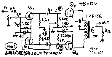
1.Old fashion fhase invertor: Fig1
Q1 acts as a normal source grounded amplifier. The output signal of it
is injected on the gate of Q2 after divided by 5k ohms potentiometer. Q2
workes also as a normal source grounded amplifier. Source grounded amplifier
sifts the phase of the signal. Therefore the output signal of Q2 has the
inverted phase from the output signal of Q1. I had to tune the potentiometer
in order to chancel the amplitude by Q2 with the dividing factor of the
potentiometer. I adjusted the potentiometer to minimize the strain factor
of the output signal of the amplifier ,useing the handmad strain meter
indicated on the another page of my homepage. After tuning, I examine the
performance of this amplifier. See the following data! Not "Jody",
but "Data".
ppamp1.gif----Right side of (A) and (B) point of Fig1 is the common of
all this pages.
| input siganl |
output siognal |
gain |
strain |
power |
| mVc-p |
mVc-p |
dB |
% |
mW |
| 40 |
50 |
1.9 |
0 |
0.16 |
| 70 |
100 |
3.1 |
0 |
0.63 |
| 130 |
200 |
3.7 |
0 |
2.5 |
| 220 |
300 |
2.7 |
2.5 |
5.6 |
| 200 |
400 |
2.5 |
5 |
10 |
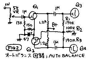
2.Automatic balanced circuit : Fig2
This circuit is same as the last circuit, as the output signal of Q1 is
injected on the gate of Q2 after divided by the R1 and R2 divider. But
, in this circuit, the output signal of Q2 is also divided by the R3 and
R2. And it was injected on the gate of Q2. Therefore the Q2 acts as a highly
negative feed back inverting amplifier. Therefore the gain of Q2 amplifier
becomes odB automatically. This is the theory of this " automatic
balanced circuit". But the actual performance was far from the name
of it. See the data!
ppamp2.gif
| input |
output |
gain |
strain |
power |
| mVc-p |
mVc-p |
dB |
% |
mW |
| 35 |
50 |
3.1 |
0 |
0.16 |
| 70 |
100 |
3.1 |
1 |
0.63 |
| 150 |
200 |
2.5 |
7.5 |
2.5 |
| 280 |
300 |
0.6 |
17 |
5.6 |
| 500 |
400 |
-1.9 |
50 |
10 |
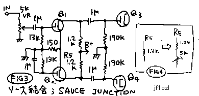
3.Source connected phase inverter:Fig3
On this circuit, the source of Q2 is connected on the source of the Q1.
The gate of Q2 is grounded by the capacitor,1 micro farad. Q2 acts as the
gate grounded amplifier. The gate grounded amplifier inverts the phase
of the signal. Therefore the Q2 acts as the phase inverter. See the performance
data! This type of amplifier has the very big strain factor,because the
Q2 has minus gain. And the level of a pair of signals is not the same.
I changed the R2,the load resister of the Q2 from the 1.2k to 5k ohms potentiometer.
And I adjusted to minimize the strain of the amplifier. See the improved
performance of this type of amplifier!
ppamp3.gif -----SAUCE is spell miss of source,.
 Prformance
of Fig3:
Prformance
of Fig3:
Performance of an
Original Source connected Fhase invertor
| imput |
output |
gain |
strain |
power |
| mVc-p |
mVc-p |
dB |
% |
mW |
| 60 |
50 |
-1.6 |
0 |
0.16 |
| 120 |
100 |
-1.5 |
3.5 |
0.63 |
| 260 |
200 |
-2.3 |
10 |
2.5 |
| 500 |
300 |
-4.4 |
25 |
5.6 |
| 800 |
400 |
-6 |
50 |
10 |
Performance of Fig4 : Performance of the improved type
| imput |
output |
gain |
strain |
power |
| mVc-p |
mVc-p |
dB |
% |
mW |
| 45 |
50 |
0.9 |
0 |
0.16 |
| 90 |
100 |
0.9 |
0 |
0.63 |
| 180 |
200 |
0.9 |
1.5 |
2.5 |
| 270 |
300 |
0.9 |
2.5 |
5.6 |
| 400 |
400 |
0 |
5 |
10 |
4.P-K divider circuit:Fig5
Q1 acts as a normal source grounded amplifier. Q2 acts as a source grounded
amplifier , when it is seen from the load resistor on the drain of it.
And ,on the same time, Q2 acts as a source follower amplifier , when it
is seen from the load resistor on the source of it. A source grounded amplifier
inverts the signal. A source follower do not change the phase of the signal.
Therefore the pair of signals has opposite phase from each other. See the
performance data! This type of amplifier has a good performance, low strain.
I will give you a home work. Connect the Q1 and Q2 direct without any capacitor!
I had shown the type of circuit on the Japanese CQ magazine on 1993 September.
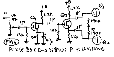
performance of Fig5
| imput |
output |
gain |
strain |
power |
| mVc-p |
mVc-p |
dB |
% |
mW |
| 40 |
50 |
1.9 |
0 |
0.16 |
| 80 |
100 |
1.9 |
0 |
0.63 |
| 160 |
200 |
1.9 |
0 |
2.5 |
| 250 |
300 |
1.9 |
1.5 |
5.6 |
| 400 |
400 |
0 |
15 |
10 |
ppamps.gif-----comparison of the strain charactor of some phase inverter
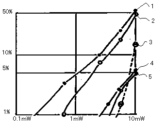 1.Source
connected phase invertor "without tuning"
1.Source
connected phase invertor "without tuning"
2.Automatic balanced inverter "without tuning"
3.P-K divider
4.Source connected phase invertor "with tuning"
5.OLd fashion phase invertor "with tuning"
In any type of invertor, tuning must be done!!
プッシュプル増幅器の位相反転器の比較研究
中学生の頃、ちょうどトランジスターの実用化時期に差し掛かった頃に、まだ大きな電力を扱うアンプの主力は真空管でした。私は雑誌で、プッシュプルアンプ
には多くの位相反転回路が実用されている事を学びましたが、道端で拾ってきたラジオは、皆30A5や47のシングルの電力増幅器を使っていて、プッシュプ
ル増幅器というのは、本でしか見れない「高嶺(たかね)の花」でした。時が流れて、会社に入って、結婚して、子供ができて、会社の後輩が有線テレビの「ス
タートレック」という番組(アメリカのSF)をビデオにとって見せてくれる様になると、その中に、”ジョディー”という登場人物が”フェーズシフター”な
る機器を調節する場面が頻繁にでてきました。人の話によると、この”スタートレック”の監督はロッデンベリーさんというアマチュア無線家だそうです。そこ
で、私は、ちいさい頃のあこがれだった、位相反転回路すなわちフェーズシフターに関して、試作、試験してみる事にしました。ただし、真空管で実験するのは
経済的にも大変なので、真空管と同じ動作原理すなわち「電圧入力ー電流出力」のFETで作ってみました。
位相反転器には、古典的回路、自動平衡回路、カソード結合回路、PーK分割回路が代表的な4種類です。この4種類を順番にためしてみました。尚、全ての
FETは、 2SK192A-Y, I dss=3mA
を使用しました。これは、高周波用のきわめて電流の小さなFETですので、出力電力は本当に小さいです。私自身が、1993年9月のCQ誌に紹介した様
に、ここに、低周波増幅用のもっと電流な大きなFETをもってきて、パラレル接続等すれば、1W程度の出力が確保可能です。
1.古典的回路:図1(FIG1)
Q1は普通のソース接地増幅器として動作します。その出力はQ3のゲートに加えられると同時に、(A)点とグランドの間に入った5kオームの抵抗で分圧さ
れて、反転管(石)Q2に入力されます。Q2はやはり普通のソース接地増幅器として動作します。この増幅器は増幅と同時に位相を反転するので、Q2のドレ
インには反転された信号が出てきます。ここで、Q2の増幅率と同じ大きさになるように、(増幅を相殺する様に)、先ほど出てきた5kのポテンショの分圧比
を調節すれば、(A)点と(B)点の信号は振幅が同じで、位相が反転した信号になりますので、その後のプッシュプル増幅器であるQ3とQ4を逆位相で駆動
できます。これが一番簡単で基本的な位相反転回路なので、古典的回路と呼ばれています。実際には、増幅器の出力自体の歪みが最小になる様に、5kオームの
ポテンショメーターを、調整しました。
図1の回路における、入力電圧、出力電圧、利得、歪み、出力電力等の実測値を計ってみたのが下の表です。
ppamp1.gif−−−−(A)点と(B)点から右側はこのページの全ての回路図において共通です。
| 入力電圧 |
出力電圧 |
利得 |
歪み |
出力電力 |
| mVc-p |
mVc-p |
dB |
% |
mW |
| 40 |
50 |
1.9 |
0 |
0.16 |
| 70 |
100 |
3.1 |
0 |
0.63 |
| 130 |
200 |
3.7 |
0 |
2.5 |
| 220 |
300 |
2.7 |
2.5 |
5.6 |
| 200 |
400 |
2.5 |
5 |
10 |
2.自動平衡回路:図2(FIG2)
次に作ってみたのが、自動平衡回路です。この回路も、Q1で増幅した信号をR1=190kとR2=100kで分圧して、Q2のゲートに入力する所までは、
先ほどの古典的回路と同じなのですが、Q2の出力であるドレインの信号が、もう一度R3=190kとR2=100kで分圧されて、Q2の入力に入るように
なっています。ここで、Q2は反転増幅器であり、その入出力がつながっているという事は、すなわち、Q2には、強力な負帰還がかかっていて、Q2の増幅率
は自動的に1倍に保たれています。このため、この回路はQ1とQ2の振幅が同じ大きさにそろうので、自動平衡回路と呼ばれています。
図2の回路における、入力電圧、出力電圧、利得、歪み、出力電力等の実測値を計ってみたのが下の表です。
自動平衡回路という割りには全然自動的に低歪みになっていません。先ほどの、古典的回路では出力自体の歪みが最小になる様に、調整した結果ですので、「調
整した古典的回路の方が、調整しない自動平衡回路よりマシ」である事がわかります。これは単に位相反転回路だけの問題では無く、先ほど古典的回路の調整の
際には、プシュプル回路のQ3とQ4のアンバランスを含めて、歪み最小に調節されている事が原因であろうとおもいます。
ppamp2.gif
| 入力電圧 |
出力電圧 |
利得 |
歪み |
出力電力 |
| mVc-p |
mVc-p |
dB |
% |
mW |
| 35 |
50 |
3.1 |
0 |
0.16 |
| 70 |
100 |
3.1 |
1 |
0.63 |
| 150 |
200 |
2.5 |
7.5 |
2.5 |
| 280 |
300 |
0.6 |
17 |
5.6 |
| 500 |
400 |
-1.9 |
50 |
10 |
3.ソース結合反転回路:図3(FIG3)
次に、真空管のカソード結合に相当するソース結合を作ってみました。Q1のソースとQ2のソースは直接つながっています。またQ2は、ゲートが1μのコン
デンサーで交流的に接地されているので、Q2はゲート接地増幅器として動作します。ゲート接地増幅器は、位相を反転するので、Q2は位相反転回路として動
作します。
図3の回路における、入力電圧、出力電圧、利得、歪み、出力電力等の実測値を計ってみたのが下の表です。
ppamp3.gif
| 入力電圧 |
出力電圧 |
利得 |
歪み |
出力電力 |
| mVc-p |
mVc-p |
dB |
% |
mW |
| 60 |
50 |
-1.6 |
0 |
0.16 |
| 120 |
100 |
-1.5 |
3.5 |
0.63 |
| 260 |
200 |
-2.3 |
10 |
2.5 |
| 500 |
300 |
-4.4 |
25 |
5.6 |
| 800 |
400 |
-6 |
50 |
10 |
という、具合で、何と出力電力で1mWいかない内から、歪みが発生してしまいます。オシロスコープでQ1とQ2の出力を観察してみると、Q2の出力のほう
が半分くらいになっています。ゲート接地は、作りっぱなしでは、決して振幅が1倍になりません。そこで、図4のように、Q2の負荷抵抗を5kオームのポテ
ンショメーターに変えて、Q1とQ2の出力を観察しながら、Q2の出力がー1倍になるように調整したのが下の表です。歪みは、これでだいぶ改善されまし
た。歪みと出力の関係を、見やすくグラフにしたのが、図5(FIG5)に示しましたので、下の表を見てください。
| 入力電圧 |
出力電圧 |
利得 |
歪み |
出力電力 |
| mVc-p |
mVc-p |
dB |
% |
mW |
| 45 |
50 |
0.9 |
0 |
0.16 |
| 90 |
100 |
0.9 |
0 |
0.63 |
| 180 |
200 |
0.9 |
1.5 |
2.5 |
| 270 |
300 |
0.9 |
2.5 |
5.6 |
| 400 |
400 |
0 |
5 |
10 |
4.P−K分割方式位相反転回路:図5
図5において、Q1はただのソース接地増幅器です。Q2はドレインとソースに同じ負荷抵抗がつながっているので、ドレイン側の出力としてはソース接地とし
て動作し、ソース側の出力としてはドレイン接地として動作するという事になっています。ドレイン側の出力はゲートからの入力信号を反転出力し、ソース側の
出力は非反転出力なので、Q2の二つの出力は互いに位相が逆になります。この回路の成績を下の表に示します。
ppamp5.gif
| 入力電圧 |
出力電圧 |
利得 |
歪み |
出力電力 |
| mVc-p |
mVc-p |
dB |
% |
mW |
| 40 |
50 |
1.9 |
0 |
0.16 |
| 80 |
100 |
1.9 |
0 |
0.63 |
| 160 |
200 |
1.9 |
0 |
2.5 |
| 250 |
300 |
1.9 |
1.5 |
5.6 |
| 400 |
400 |
0 |
15 |
10 |
図5、FIG5,:各回路の、歪みー出力の比較ーーーーーppamps.gif
1:ソース結合(無調整)
2:自動平衡(無調整)
3:P−K分割
4:ソース結合(調整後)
5:古典的回路(調整後)
いかなる回路であろうとも、調整無しでは歪みは大きい。
逆に、古典的回路でも、ちゃんと調整した後は歪みが少ない。
back to index
