The brilliant "miniVFO"
A simple, cheap, tiny, rock steady 3-30MHz VFO
Designed by sv3ora

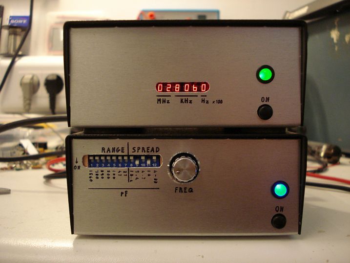
The minivfo (below) used as an RF signal generator and combined with my MCU-free frequency counter (above)

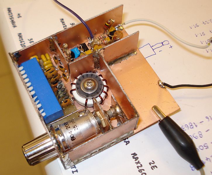
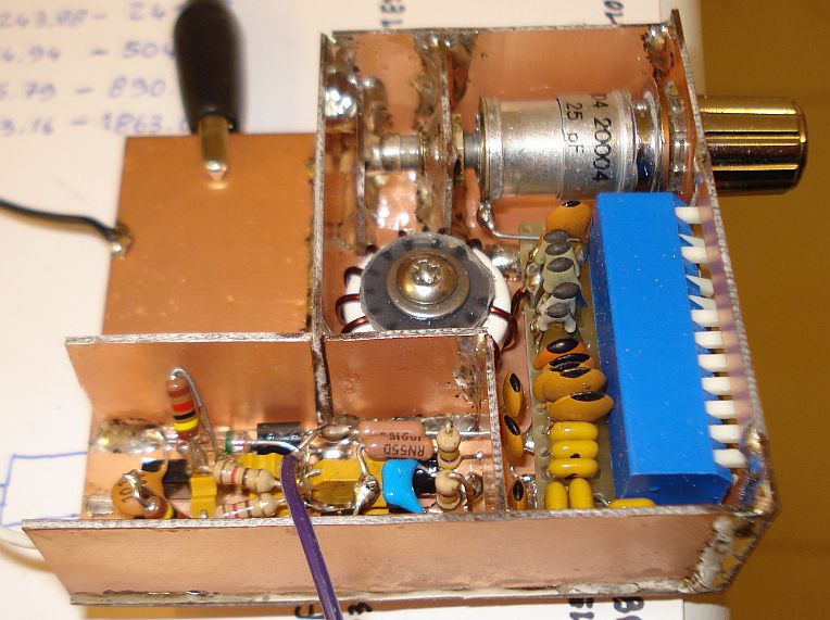
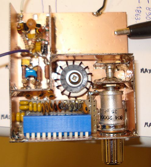
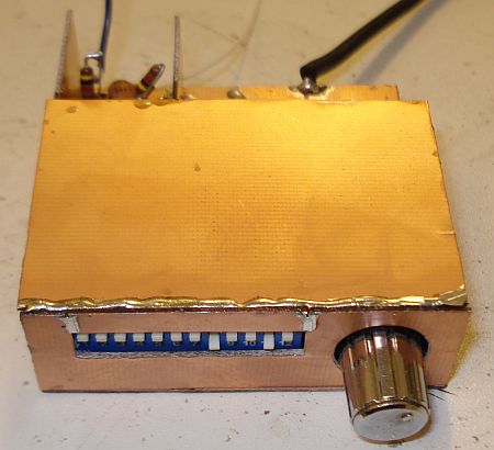
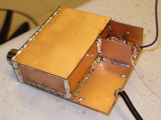
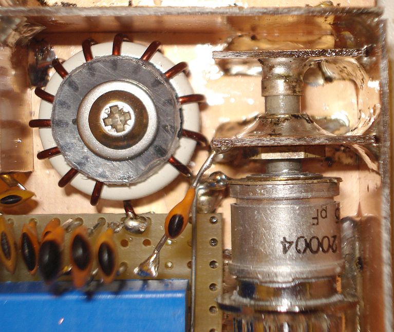
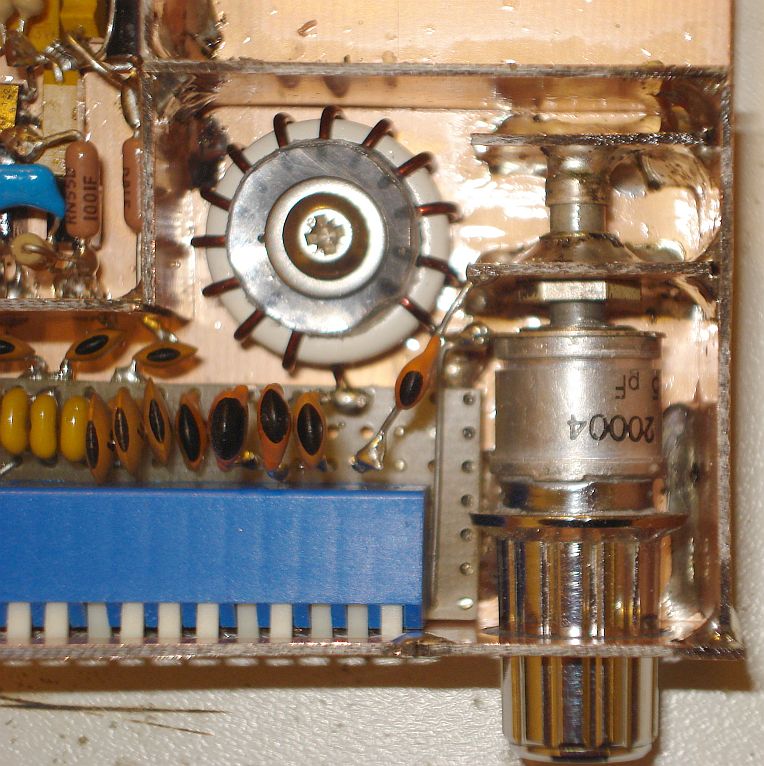
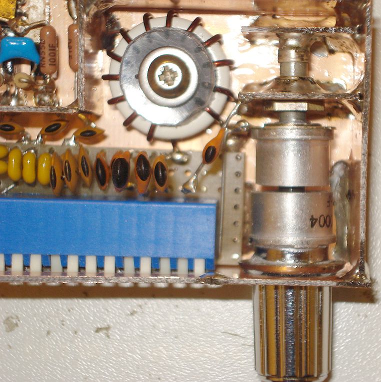
The minivfo internals

In the past I have built and tested many crystal oscillators for my projects. I have also built broadband crystal oscillators, in the sense that the crystal was the only component required to be changed for a different frequency or band of operation. These circuits work well and they are stable, but there is a need to obtain crystals for in-bands operation and these crystals are harder to find and expensive. Even then, you are restricted to operate on specific frequencies only, plus or minus a very small range around the crystals (VXO). These days, where fewer and fewer people seem to use shortwave, your chances to make QSOs when operating only on specific frequencies, may be very limited, especially when transmitting QRP. To be honest, I rarely had great QSO success when calling on a frequency, waiting for any answers. I mostly find good signal stations and try to reach them. These stations rarely transmit on the available crystal frequencies. Remember, in most cases the frequency of a VXO cannot be varied a lot especially in the lower bands. A few KHz out and you completely miss the signal. And you also have to allow for some tunning to be able to hear a comfortable tone when operating CW or to zero beat an SSB station. So despite crystals are very stable in frequency, their use is very limited.

The next frequency-stable and promising solution is to use a DDS oscillator. Nowadays, with the improvements in DDS technology, a digitally-synthesized frequency-stable wideband oscillator with good characteristics can be made at very low cost. It almost makes no sense to try to build an analogue type VFO, commonly composed of many resonators, so as to cover a wide frequency range. But for the homebrewer, the situation may be quite different. There are various reasons for that. The DDS requires a microcontroller in order to set it's frequency. The microcontroller requires a programmer hardware and software, in order to be programmed. A PC is also required for the programming operations. Quite a few of the homebrewers do not know how to write a program to control the DDS and learning MCU programming is difficult for many. Thus, they rely on programs others have built and they cannot alter their operation to their needs. Any bug in the program can immediatelly stop your project. The DDS also requires a stable very high frequency clock oscillator for it's operation although the situation becomes a bit better (lower frequency needed) if there are internal frequency multipliers within the DDS chip. Apart from these things, soldering a DDS chip is a nightmare for the homebrewer with little or no experience in SMD and it requires SMD equipment. The tiny pinout of the DDS chips can be proven to be challenging to solder, even for more experienced people and prototyping is almost out of question. Finally, a DDS chip is a "black box" module and there is no real satisfaction to the RF experimenter, since he is not building any RF circuit, but just using a chip to produce the RF without any chance to change it's RF characteristics. Take the time to read the list of requirements in this paragraph and you will immediatelly see why a DDS-based oscillator is not always the best solution, practically speaking. Even the cost of the DDS chip that might initially be thought as low, can be proven to be much higher at the end, with all those mentioned requirements. A DDS oscillator project is also generally considered a complex project requiring quite a lot of parts, some of them not in the average homebrewers junk box.

Another solution for a stable variable frequency oscillator, is to use an analogue varicap-controlled VFO and phase lock it to a reference crystal oscillator. The old MC145151 is one of the simplest PLLs I am aware of. It requires a microcontroller for quick frequency changing or a set of a few CMOS or TTL chips, to change it's frequency. Some extra switching is needed as well, to switch the VFO resonators for different bands. This chip can be controlled by DIP switches as well, without the need for the extra chips, but setting a frequency requires some calculations from the user each time, so scanning a band for signals is out of question. Again it is considered a more complex project requiring quite a few parts.

The VFO stabilizer is another option for a stable variable frequency oscillator. It uses an analogue varicap-controlled VFO and a frequency comparator to achieve the same effect as that of the PLL. There are two modes of operation, the slow and the fast mode. In the faster mode a stable high frequency clock is required and even then, the stability is not guaranteed on higher bands. It is also considered a more complex project requiring quite a few parts.

The simplest solution, requiring the least number of parts, seems to be an unlocked VFO. But most unlocked VFOs are not stable enough for SSB/CW operation. That is the main reason why all the previously mentioned solutions have been invented. However, there are a few VFO circuits on the literature that claim to be very stable in frequency. Most of these designs have limited tuning range. Some of them, utilize temperature-compensation by using special components that compensate for the temperature-related frequency drift of the oscillator. Temperature compensation is difficult to achieve and it is not easily reproduced. Some other VFOs achieve frequency stability by other means. The oscillator I describe in this article, is such.


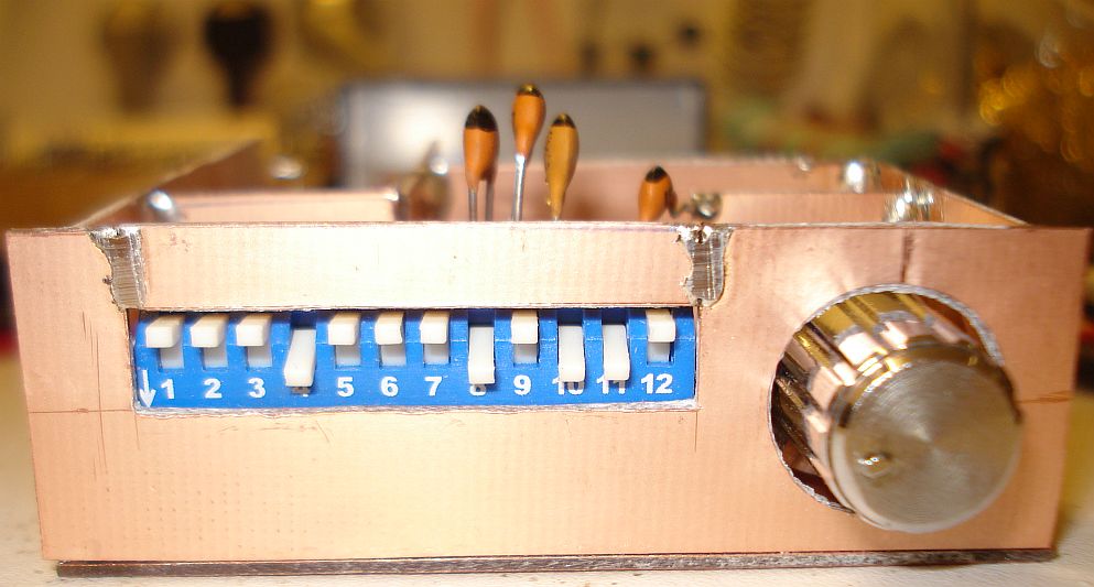
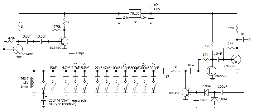
DIP switch settings notes:

All the capacitors are switched in a "decade capacitor" way. So when for example you close the switches of 100pF and 47pF, you have a total capacitance of 147pF.

The first switch close to the variable capacitor is used when full trimmer capacitance is needed (usually on lower bands). This switch is open and the 10pF one is closed, when only a part of trimmer capacitance is needed (spread), usually on higher bands or on lower bands to achieve greater span. The next three capacitors (4.7-6.8pF), are used to select the different segments of the spreaded trimmer capacitance. The final seven capacitors are used in lower bands, where span is adequate without the nead for any spread. However if greater span is needed in lower bands, the
4.7-6.8pF capacitors can be used in combination with these seven capacitors.

Note, the miniVFO will operate even outside the HAM bands. There is lot of overlap in the capacitance and spread ranges, so that continuous coverage of 3-30MHz is achieved.

The complete schematic of the miniVFO is shown in the picture above. It is as simple as that and it will give you rock-stable variable frequency operation at all HF frequencies (not only specific bands) and so it can be used reliably for your HF transceivers. It has some interesting features not easily met in other VFO designs:
The circuit is built around the Franklin VFO topology. Any tunable oscillator consists in essence of two parts, a tuned circuit of high Q and a maintaining amplifier to replenish the losses in the tuned circuit. A basic advantage of the Franklin oscillator is that the maintaining circuit need to be only very loosely coupled to, and impose very light loading of the resonant circuit. Another practical advantage is the single two-terminal coil, without taps, which has one end at RF earth (also true for the variable capacitor), with no capacitive or inductive divider as in the Hartley or Colpitts circuits and most of their variants, which is frequency conscious. Because of the loose coupling, those changes affecting the maintaining amplifier, whether valve or solidstate, are arranged to have only very limited effect on the frequency.


It is important to remember that the stability of a Franklin oscillator depends upon the quality of the frequency-determining high-Q LC resonant tank circuit and the looseness of the coupling to it. Thus, the coupling capacitors must be the smallest possible that ensure reliable start up of the oscillator at all frequencies of interest.

My miniVFO" is built around this topology. As can be seen in the schematic, the coupling capacitors of the resonant circuit to the active devices are only 3.3pF each. These capacitors, but also all the frequency-determining capacitors of the miniVFO (switched capacitors and 470pF inter-stage coupling capacitor), must be of NP0 ceramic type, so as to provide temperature immunity for the oscillator, which leads to even more frequency stability. My previous experiments on oscillators, have proven that the cleanest point (purest sinewave) to extract the signal out of any oscillator, is the resonator point. Thus, in contrast to all the other Franklin oscillators I have seen, I extract the output of this oscillator directly from the LC resonators. This has the disadvantage of course, that the LC is loaded more. But practically speaking, I placed a 3.3pF capacitor at the LC to couple energy out and I did not find any significant loading of the LC. I guess it could have been done also without any coupling capacitor, using just a separate coupling winding near the L, but I thought the coupling capacitor method to be easier and more easily reproduced with similar results each time, because it does not depend on the style of the winding from the builder.

The output level of any Franklin oscillator is very low and in my oscillator, where I couple the output directly from the LC using a very small value of coupling capacitor, this level is even lower. To be usable and also to ensure frequency stability under different loads, the VFO needs a good buffer. In the past, I have designed a small buffer based around a 2N2222 transistor, that is easy to build, broadband, does not require a transformer, can drive 50 ohm loads and has a low harmonics content in the range of -35dBc to -40dBc. To bring the level of the VFO to around 5mW, I cascaded two such amplifiers, based on the cheap plastic versions of the 2N2222 BJTs.
The buffer amplifiers draw almost 60mA.

To make the level of the VFO more constant at all frequencies, I tested an ALC loop that I had previously used in audio circuits, but now applied to the RF. It is essentially an automatic potentiometer, which works flawlessly in this VFO.

It is important for the power supply to be able to provide a stable voltage to the oscillator section of the miniVFO. This is accomplished by the use of a linear regulator. It could be made discrete, but linear regulators are very comon nowadays and I thought it would not worth the extra components needed for a discrete circuit. The 5V regulator can be the 78L05 (TO-92 package) or the standard 7805 (bigger package).

One of the most interesting things about this VFO is that for covering its whole range (3-30MHz) only a single untapped inductor is needed and a few switched capacitors (which must be all NP0/G0G !!!). This makes it really easy to build, cheap and small-sized. As far as concern the switched capacitors, for lower cost, only seven different capacitor values are used in the DIP switch and the bigger capacitors are composed by combining lower value ones. The capacitor values have been chosen with great care, so that there are no capacitance gaps and there is adequate overlap. Also, other things had to be taken care. For example at higher bands, where tiny variable capacitance changes cause much greater frequency changes, a network of switched capacitors was used to split the variable capacitor range into smaller fractions (with adequate overlap), each of these fractions selected by combining three switched capacitors. Just for reference, below are these three capacitors combinations.

Series capacitor along with variable capacitor and three left caps combinations:

varcap+series10pF                       Variable capacitor alone
2.86-7.67
pF              

(varcap+series10
pF)+4.7pF               a      4.7pF    (=4.7pF)
7.56-12.37
pF  

(varcap+series10
pF)+9.4pF               b      9.4pF    (=4.7pF+4.7pF)
12.26-17.07
pF  

(varcap+series10
pF)+4.7pF+9.4pF         a+b    4.7pF+9.4pF
16.96-21.77pF  

(varcap+series10
pF)+13.6pF              c      13.6pF   (=6.8pF+6.8pF)
16.46-21.27
pF  

(varcap+series10
pF)+13.6pF+4.7pF        c+a    13.6pF+4.7pF
21.16-25.97pF  

(varcap+series10
pF)+13.6pF+9.4pF        c+b    13.6pF+9.4pF
25.86-30.67pF  

(varcap+series10
pF)+13.6pF+4.7pF+9.4pF  c+a+b  13.6pF+4.7pF+9.4pF
30.56-35.37pF


This split capacitance mechanism can be used on lower bands too to "zoom in" a specific segment of a band. Quite a few days worth of calculations have been made for this to be possible, so do not change their values unless you are really sure how this works.

As far as concern the inductor, the frequency stability is more than adequate at all frequencies using this single inductor alone. Build this inductor exactly as I did, with 13 turns of 1mm diameter enameled copper wire, evenly spaced around a T68-7 toroidal core. This will guarrantee you similar results as mine. Go ahead and experiment with other cores and coils if you like, but do not judge the frequency stability of your version of the miniVFO, based on your particular inductor, if it is not built as I describe. Keep the leads of the inductor short. You can also keep it firm by attaching it with a non-magnetic screw and a few pieces of plastic onto the PCB of the VFO as I did it, trying to keep it away from magnetic metals.


The completed miniVFO internals, are shown in the picture above. Notice the strong RF shielding of the resonating components from the rest of the circuit. This shielding is made out of small pieces of double sided PCB material, cut into shape and tin soldered together. Both sides of the PCB must be grounded, to double the effectiveness of the shield.
The shield doubles as RF, as well as a form of thermal shield. Especially the buffer amplifiers generate heat, so this heat must not be allowed to reach the resonating elements. When you solder the PCB pieces together, make sure you cover the joints with solder, so as to minimize the amount of air flow in the resonating elements cabinet. When you finish with the side walls shields and when you are satisfied with the performance of the circuit, close the top side of the circuit with a lid shield as well (not shown here for demonstration purposes). Shielding is very important for any VFO design, so make sure you keep the VFO resonating elements as isolated as possible.


Even with this strong shielding I used, there are some minor hand effects, primarily in the higher frequencies. These hand effects are caused by the little opennings of the DIP switches. However, as you move your hand half a centimeter or so away from the DIP switch, these hand effects disappear.


The front panel of the miniVFO is shielded the same way. A few openings have to be done for the DIP switches and the knob of the variable trimmer capacitor. Make sure you make these openings as small as possible, to minimize hand effects. Notice the four NP0 spread capacitors that extend from the miniVFO. These were placed temporarily there (when I took the first pictures of the miniVFO), to experiment with different spread settings. In the final version when the lid shield of the miniVFO will be put in place, these capacitors must lie inside.

There are primarily two things that make possible for this VFO to be minutarized. The first, is the use of a single inductor and the tiny DIP switch for switching the different static capacitors, which is configured in a decade capacitor configuration, to minimize the maximum number of capacitors needed.


The second, is the use of a variable air trimmer capacitor instead of the bigger air types. This trimmer has a much smaller maximum capacitance but also a much smaller minimum. Combined with the switched decade capacitor network, a composite larger capacitance is achieved, which is actually much larger than any big variable capacitor would allow. And all the above at minimum physical volume. With this decade capacitor and trimmer combination, a 4pF to about 3.1nF composite variable capacitor is achieved, a range not practical with any single big variable capacitor.

However, the use of this approch, splits the lower bands into segments. So it might be annoying to have to switch a few DIP swithes to cover another band segment on 80m. However, this could be thought as an advantage, as the tuning precision (spread) increases. In the higher bands the use of the small capacitance trimmer comes actually to a great advantage, as tiny capacitance changes are only required to tune these bands. In fact for these bands, the combination of the trimmer capacitor and the three spread capacitors (left hand side of the DIP switch in the schematic) is actually mandatory, to decrease the capacitance range even more and increase the tuning spread.


The most impractical thing when using these small variable air trimmers as the main tuning element, is the lack of a shaft to tune them with front panel knobs. A specific type of these trimmers, shown in the photo above, is called "beehive" variable capacitor and you can find them also as "tubular" or "piston" variable capacitors. Despite they are of low total capacitance (like all trimmers), they are small in size compared to their big brothers, they have high-Q, they can handle quite a lot of power and voltage (500V), they are relatively cheap, and due to their construction, they are always finely-tuned, since they all have an embedded mechanical reduction drive (their screw)! I have found these trimmers to be backlash-free as well, which means that as you tune back and forth you do not skip frequencies due to backlash. This is very important when tuning around. Whereas in a standard trimmer the usable rotation is half turn at maximum, these trimmers have several turns to achieve the same capacitance variation. And all these, at very low cost compared to their large and bulky brothers, excellent!

Moreover, these particular types of trimmers, allow a knob to be easily soldered onto them, because there is a big surface for the knob to be soldered in contrast to the little delicate screws other types of trimmers have. See the pictures above and notice how I soldered a knob directly onto the "rotor" portion of the beehive trimmer. Just make sure the inner hole of the knob is wide enough to fit in the screw of the trimmer and long enough so that it does not prevent the plates from being fully pushed inwards to achieve maximum capacitance. A possible drawback is that your front panel knob is pushed in and pulled out when tuning the trimmer. Also there is no screw to attach these trimmers to the front panel.

Both of these disadvantages can be eliminated as shown in the pictures. Instead of screwing the trimmer on the front panel, I usually use a small piece of PCB and solder the back of the trimmer on it. But if you notice closely the miniVFO pictures, I actually used two pieces of PCB and soldered the two available back points of the trimmer, to allow for greater mechanical stability. If your particular trimmer has just one point instead, solder a single piece of PCB instead. The PCB pieces are put at a distance from the back of the front panel and so, the soldered trimmer stands behind the panel and perpendicular to it. Then I do a hole in the panel from which the knob (soldered onto the trimmer) extends through. The knob is not attached or touching the front panel, it just passes through the hole and extends from it.


This approach works fine, but there is a drawback. You do not know when to stop unscrewing the trimmer, so you may accidentally remove the top cap ("rotor") from the rest of the trimmer body. The solution I found, is to use a knob with a ring-shaped body at its end. The hole on the panel is made as large as the knob handle, but smaller than the diameter of the ring at the end of the knob. When the trimmer is fully unscrewed, the knob ring will reach the panel surface and it will act as a stopper, preventing from further unscrewing of the knob. Before permanently soldering the back side PCB (that holds the trimmer body) in place, unscrew the trimmer fully so that you can set the desired stop point. Then solder the PCB in place permanently. That way, you can also define a different predetermined minimum capacitance for your trimmer if you like.

The picture above, shows the trimmer fully screwed in (maximum capacitance). The knob passes through the front panel hole and extends only a little out of it.
The picture below, shows the trimmer fully unscrewed (minimum capacitance). The knob passes through the front panel hole and extendeds fully out of it. The ring on the knob body, touches the front panel PCB and stops the trimmer from further unscrewing.


Back to main site