A homemade minicomputer made entirely out of TTL ICs for educational purposes
This project is not complete yet. Do not rely on the information on this page to build the computer.

Preface | Overview | Clock and micro-instruction logic | Arithmetic logic unit | Memory and addressing | Input / Output | Programming Interface | Sample Programs | Enclosure | PCB artwork | Manual EPROM programmer
This project is a 4 bit CPU built from TTL counters, latches and gates. Two, 2716 EPROMs are used to store the micro-instruction code and two, 2114 static RAMs are used for program memory. 25 ICs in all. This project is meant to be more educational than be a practical, useful CPU. The design is simple and can be built from readily available TTL ICs.
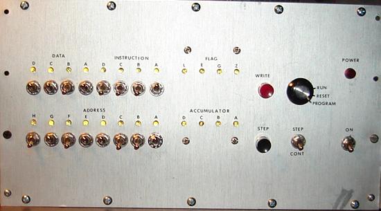
The programming and control interface is the classic toggle switch / LED type as was the Altair 8800 and IMSAI 8080 microcomputers of the 1970s. This type of interface is simple to design and build. Programming the CPU with this sort of interface isn't as difficult as one may think.
There are three modes of operation set by a rotary switch. These are Program, Reset and Run. For program mode, there is a write button to write the instruction to the address that is indicated by the address toggle switches. (The other button and switch for step and step mode were installed for a previous version of the CPU and are not used here.)
Why did I do this?
I wanted to design a simple 4 bit CPU to show other electronics hobbyists that designing and building a simple CPU is not difficult to do. A relatively small number of ICs is required even without using PALs or GALs. This 4 bit CPU was designed, built and tested without the aid of a logic analyzer or any hardware simulation software. I only used a logic probe and an oscilloscope.
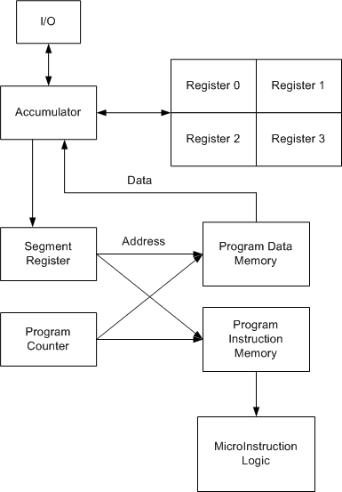
This CPU has 16 instructions. More instructions could have been implemented but 4 bit instructions means 16 is the limit. There is one accumulator and four registers. The registers are the only memory available for a program to store data at runtime. The program space is 256 bytes. 4 bits for the instruction and another 4 bits to store program data. There are three flags, less than, equal to and greater than. A segmented memory model is used. There are 16 segments of 16 bytes. The program will execute in a 16 word segment until a jump is made to another segment. This was done to simplify the design.
Here is a block diagram of the CPU -
Below is a summary of the available instructions -
| Code | Numonic | Description |
|---|---|---|
| 1 | LIT | Copy a literal value from program memory to the accumulator. |
| 2 | LOAD | Copy a value from a register to the accumulator. |
| 3 | STORE | Copy the value in the accumulator to a register. |
| 4 | INC | Increment the accumulator by one. |
| 5 | DEC | Decrement the accumulator by one. |
| 6 | REG | Copy the value in the accumulator to the register address latch. |
| 7 | CMPL | Compare the accumulator to a literal value. Sets flags. |
| 8 | CMPR | Compare the accumulator to a register. Sets flags. |
| 9 | RST | Resets the program counter. |
| 10 | JUMPL | Copy the value in the accumulator to the segment register when the less than flag is set. |
| 11 | JUMPE | Copy the value in the accumulator to the segment register when the equal flag is set. |
| 12 | JUMPG | Copy the value in the accumulator to the segment register when the greater than flag is set. |
| 13 | IN | Copy the value from the input to the accumulator. |
| 14 | OUT | Copy the value in the accumulator to the output latch. |
| 15 | NOP | No operation. |
As you can see, there are 15 instructions shown here instead of 16. One other instruction, FETCH, is used by the micro-instruction logic and should never be used by a program.
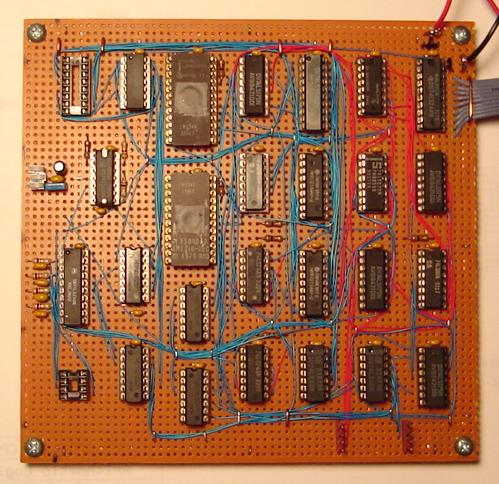
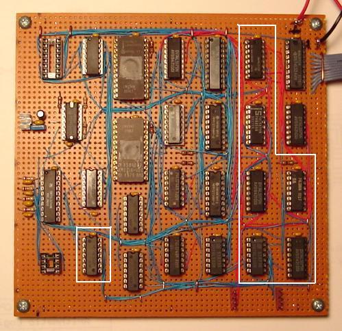
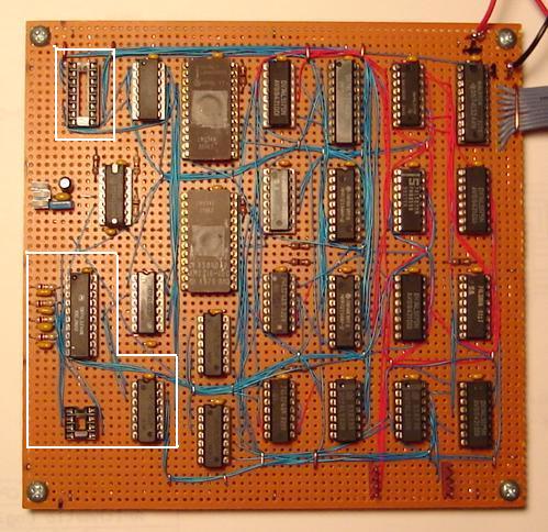
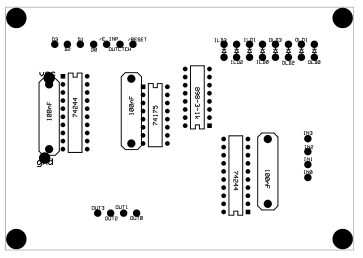
Shown above is the main circuit board. This is the CPU circuitry and does not include the programming interface. On the left hand side, there is a 16 pin DIP socket that connects to the toggle switches and LEDs for the programming interface. The 8 pin DIP socket is for control - program, reset and run mode and the write button. On the bottom, right hand side of the board are two 4 pin headers that connect to the LED buffers for displaying the flags and accumulator contents.
The schematics show generic 7400 series TTL part numbers but the CPU was actually constructed using 74LS TTL. I do not recommend using straight 7400 TTL because of power requirements and poor noise immunity, but I suppose it can be done. Switching noise can become a problem when using point to point wiring with 30 guage wire as I used. To ensure a minimum of problems with this project I recommend the following -

Clock -
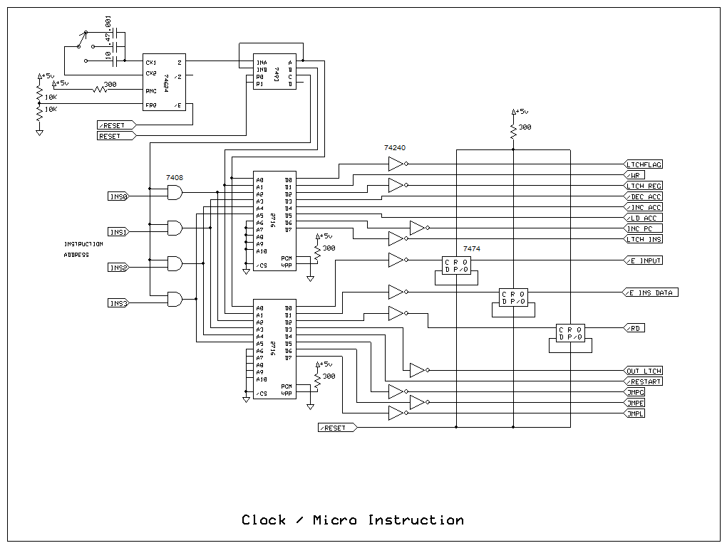
The clock is a 74LS624. This is a TTL VCO. The 74LS124 is similar and the 74LS629 is a dual VCO. I chose this IC because it has an enable input and two outputs, one output being the complement (inverted) of the other. When the the VCO is disabled (as it is in reset mode), there is no signal output. When the VCO is enabled, the first clock cycle is guaranteed to be %100 duty cycle. I'm using the inverted output to clock the CPU. This way, when reset is removed, the clock out is low for half a clock cycle. I believe this allows everything else in the CPU circuit to settle before program execution begins.
There is a three position switch to select one of three clock speeds. These clock speeds are 10Hz, 400Hz and 165kHz. The two lower speeds are meant to be used for debugging programs. The 10Hz speed allows the accumulator, flag, address and instruction values to be observed during program execution. It is difficult to verify that the CPU functions properly at 165kHz but I assume that it would.
The 74LS624 can be difficult to acquire these days. I don't think any of the TTL VCOs mentioned are in production any more. I purchased 74LS624s from a surplus outlet. I'm sure there are other oscillator / clock ICs available with characteristics similar to the 74LS624.
Sequencing -
A 74LS93 is used for sequencing the micro-instruction logic in the 2716 EPROMs. The code for each instruction is four, 16 bit words. A program is composed of instructions. However, the CPU needs to know how to execute these instructions and this is called micro-instruction logic, or micro-instruction code. This code is stored in the EPROMs. Each time a program instruction is executed, four of these 16 bit words of micro-instruction code is executed. The outputs of the EPROMs are used to control the switching in the CPU and this will be discussed more later.
The first group of micro-instruction code, at addresses 0 through 3, is the program instruction fetch code. The fetch instruction retrieves the program instruction from program memory. The fetch instruction is always executed before every program instruction to fetch the instruction from program memory. The fetch instruction should never be called from a program, it is to be used only internally by the CPU. The remaining CPU instructions are located at addresses 4 through 7, 8 through 11, etc...
When the ripple counter (74LS93) counts, the two least siginificant bits, A and B, which are connected to the address lines A0 and A1 of the EPROMs, cycle through one of the four, 16 bit word micro-instructions. Counts 0 through 3 execute the fetch instruction. During the next four counts, the C output of the counter is high. The C output is connected to a group of four AND gates. This enables any code on the inputs of the AND gates to be present on the EPROM address lines A2 through A5 (they are otherwise 0). The code at the inputs of the and gates (shown INS0 through INS3 on the schematic) is the program instruction code from program memory. The program instruction codes are used as an offset to select the proper group of four, 16 bit micro-instruction codes.
So, to summarize, the first counts (0 - 3) executes the fetch instruction to fetch the program instruction and the next counts (4 - 7) execute the program instruction. The process is repeated again at counts 8 - 11 and 12 - 15. Since the D output of the counter isn't used, it doesn't matter what value it holds, the outputs A, B and C cycle the same way.
The outputs of the EPROMs are connected to various ICs in the CPU circuit. These are count up, count down and load inputs on the 74LS193 being used as an accumulator, latch inputs on various 74LS175 latches and so-on. Some of these lines are active high and need to be kept in the low state until needed. This brings us to why there are inverters on many of the EPROM outputs.
I am probably using the 2716 EPROMs in a way they are not supposed to be used. I chose the 2716 because there many of them on the surplus market and can be salvaged from old discarded PC peripherals, as I have done. Anyway, when an output line on the 2716 is held low for more than one count cycle (by containing zeros), there is a glitch on the output when the address is changed. This glitch looks like this on an oscilliscope -
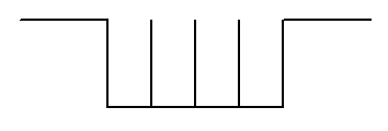
Of course these glitches cause swithing in the CPU when it is not desired. The glitches are not present when the EPROM output is held in a high state. So, the solution to the problem is to keep all EPROM outputs high. When an output needs to be low for one clock cycle, an inverter is put on the output.
I emphasize "one clock cycle". Sometimes one of the outputs needs to be low for three clock cycle (during memory and register loads to the accumulator). Holding the EPROM output low for three clock cycles re-introduces the glitches. The solution I used for this problem are flip-flops. 74LS74 flip-flops are clocked on and off producing a glitch free, three cycle low output.
Connections to other schematics -
Here is a listing of the connections to other schematics.
| RESET | Active high reset. |
|---|---|
| /RESET | Active low reset. |
| INS0 through INS3 | Instruction code from program memory. |
| LTCHFLAG | Active high signal to latch the flags into the flags register. |
| /WR | Active low signal to write the accumulator to a register. |
| LTCH REG | Active high signal to latch the register address into the register address latch. |
| /DEC ACC | Active low signal to decrement the accumulator. |
| /INC ACC | Active low signal to increment the accumulator. |
| /LD ACC | Active low signal to load the accumulator. |
| INC PC | Active high signal to increment the program counter. |
| LTCH INS | Active high signal to latch the program instruction into the instruction latch. |
| /E INPUT | Active low signal to enable input lines on the data bus. |
| /E INS DATA | Active low signal to enable program data on the data bus. |
| /RD | Active low signal to enable the selected register on the data bus. |
| OUT LTCH | Active high signal to latch the accumulator into the output latch. |
| /RESTART | Active low signal to reset the program counter. |
| JMPG | Active high signal to latch the segment register when the greater than flag is set. |
| JMPE | Active high signal to latch the segment register when the equal flag is set. |
| JMPL | Active high signal to latch the segment register when the less than flag is set. |
Micro-instruction code -
Here is the micro-instruction code listing for the two EPROMs -
ROM 0 is the one at the top of the schematic.
| ADDRESS | ROM 0 | ROM 1 |
|---|---|---|
| 0 | FF | FF |
| 1 | 7F | FF |
| 2 | BF | FF |
| 3 | FF | FF |
| 4 | FF | FD |
| 5 | DF | FF |
| 6 | FF | FF |
| 7 | FF | FD |
| 8 | FF | FB |
| 9 | DF | FF |
| 10 | FF | FF |
| 11 | FF | FB |
| 12 | FF | FF |
| 13 | FD | FF |
| 14 | FF | FF |
| 15 | FF | FF |
| 16 | FF | FF |
| 17 | EF | FF |
| 18 | FF | FF |
| 19 | FF | FF |
| 20 | FF | FF |
| 21 | F7 | FF |
| 22 | FF | FF |
| 23 | FF | FF |
| 24 | FF | FF |
| 25 | FB | FF |
| 26 | FF | FF |
| 27 | FF | FF |
| 28 | FF | FD |
| 29 | FE | FF |
| 30 | FF | FF |
| 31 | FF | FD |
| 32 | FF | FB |
| 33 | FE | FF |
| 34 | FF | FF |
| 35 | FF | FB |
| 36 | FF | FF |
| 37 | FF | EF |
| 38 | FF | FF |
| 39 | FF | FF |
| 40 | FF | FF |
| 41 | FF | 7F |
| 42 | FF | EF |
| 43 | FF | FF |
| 44 | FF | FF |
| 45 | FF | BF |
| 46 | FF | EF |
| 47 | FF | FF |
| 48 | FF | FF |
| 49 | FF | DF |
| 50 | FF | EF |
| 51 | FF | FF |
| 52 | FF | FE |
| 53 | DF | FF |
| 54 | FF | FF |
| 55 | FF | FE |
| 56 | FF | FB |
| 57 | FF | F7 |
| 58 | FF | FF |
| 59 | FF | FB |
| 60 | FF | FF |
| 61 | FF | FF |
| 62 | FF | FF |
| 63 | FF | FF |
Details of the micro-instruction code is shown below.
Micro-instruction Code Detail
Starting at address zero and incrementing by one for each line, four for each instruction.
                                                                            /E      HEX
      LTCH INC  /LD  /INC /DEC LTCH /WR  LTCH                /RST LTCH /RD  INS  /E ROM
      INS  PC   ACC  ACC  ACC  REG  REG  FLAG JMPL JMPE JMPG PC   OUT  REG  DATA IN 0  1

FETCH 1    1    1    1    1    1    1    1    1    1    1    1    1    1    1    1  FF FF
      0    1    1    1    1    1    1    1    1    1    1    1    1    1    1    1  7F FF
      1    0    1    1    1    1    1    1    1    1    1    1    1    1    1    1  BF FF
      1    1    1    1    1    1    1    1    1    1    1    1    1    1    1    1  FF FF

LIT   1    1    1    1    1    1    1    1    1    1    1    1    1    1    0    1  FF FD
      1    1    0    1    1    1    1    1    1    1    1    1    1    1    1    1  DF FF
      1    1    1    1    1    1    1    1    1    1    1    1    1    1    1    1  FF FF
      1    1    1    1    1    1    1    1    1    1    1    1    1    1    0    1  FF FD

LOAD  1    1    1    1    1    1    1    1    1    1    1    1    1    0    1    1  FF FB
      1    1    0    1    1    1    1    1    1    1    1    1    1    1    1    1  DF FF
      1    1    1    1    1    1    1    1    1    1    1    1    1    1    1    1  FF FF
      1    1    1    1    1    1    1    1    1    1    1    1    1    0    1    1  FF FB

STORE 1    1    1    1    1    1    1    1    1    1    1    1    1    1    1    1  FF FF
      1    1    1    1    1    1    0    1    1    1    1    1    1    1    1    1  FD FF
      1    1    1    1    1    1    1    1    1    1    1    1    1    1    1    1  FF FF
      1    1    1    1    1    1    1    1    1    1    1    1    1    1    1    1  FF FF

INC   1    1    1    1    1    1    1    1    1    1    1    1    1    1    1    1  FF FF
      1    1    1    0    1    1    1    1    1    1    1    1    1    1    1    1  EF FF
      1    1    1    1    1    1    1    1    1    1    1    1    1    1    1    1  FF FF
      1    1    1    1    1    1    1    1    1    1    1    1    1    1    1    1  FF FF

DEC   1    1    1    1    1    1    1    1    1    1    1    1    1    1    1    1  FF FF
      1    1    1    1    0    1    1    1    1    1    1    1    1    1    1    1  F7 FF
      1    1    1    1    1    1    1    1    1    1    1    1    1    1    1    1  FF FF
      1    1    1    1    1    1    1    1    1    1    1    1    1    1    1    1  FF FF

REG   1    1    1    1    1    1    1    1    1    1    1    1    1    1    1    1  FF FF
      1    1    1    1    1    0    1    1    1    1    1    1    1    1    1    1  FB FF
      1    1    1    1    1    1    1    1    1    1    1    1    1    1    1    1  FF FF
      1    1    1    1    1    1    1    1    1    1    1    1    1    1    1    1  FF FF

CMPL  1    1    1    1    1    1    1    1    1    1    1    1    1    1    0    1  FF FD
      1    1    1    1    1    1    1    0    1    1    1    1    1    1    1    1  FE FF
      1    1    1    1    1    1    1    1    1    1    1    1    1    1    1    1  FF FF
      1    1    1    1    1    1    1    1    1    1    1    1    1    1    0    1  FF FD

CMPR  1    1    1    1    1    1    1    1    1    1    1    1    1    0    1    1  FF FB
      1    1    1    1    1    1    1    0    1    1    1    1    1    1    1    1  FE FF
      1    1    1    1    1    1    1    1    1    1    1    1    1    1    1    1  FF FF
      1    1    1    1    1    1    1    1    1    1    1    1    1    0    1    1  FF FB

RST   1    1    1    1    1    1    1    1    1    1    1    1    1    1    1    1  FF FF
      1    1    1    1    1    1    1    1    1    1    1    0    1    1    1    1  FF EF
      1    1    1    1    1    1    1    1    1    1    1    1    1    1    1    1  FF FF
      1    1    1    1    1    1    1    1    1    1    1    1    1    1    1    1  FF FF

JUMPL 1    1    1    1    1    1    1    1    1    1    1    1    1    1    1    1  FF FF
      1    1    1    1    1    1    1    1    0    1    1    1    1    1    1    1  FF 7F
      1    1    1    1    1    1    1    1    1    1    1    0    1    1    1    1  FF EF
      1    1    1    1    1    1    1    1    1    1    1    1    1    1    1    1  FF FF

JUMPE 1    1    1    1    1    1    1    1    1    1    1    1    1    1    1    1  FF FF
      1    1    1    1    1    1    1    1    1    0    1    1    1    1    1    1  FF BF
      1    1    1    1    1    1    1    1    1    1    1    0    1    1    1    1  FF EF
      1    1    1    1    1    1    1    1    1    1    1    1    1    1    1    1  FF FF

JUMPG 1    1    1    1    1    1    1    1    1    1    1    1    1    1    1    1  FF FF
      1    1    1    1    1    1    1    1    1    1    0    1    1    1    1    1  FF DF
      1    1    1    1    1    1    1    1    1    1    1    0    1    1    1    1  FF EF
      1    1    1    1    1    1    1    1    1    1    1    1    1    1    1    1  FF FF

IN    1    1    1    1    1    1    1    1    1    1    1    1    1    1    1    0  FF FE
      1    1    0    1    1    1    1    1    1    1    1    1    1    1    1    1  DF FF
      1    1    1    1    1    1    1    1    1    1    1    1    1    1    1    1  FF FF
      1    1    1    1    1    1    1    1    1    1    1    1    1    1    1    0  FF FE

OUT   1    1    1    1    1    1    1    1    1    1    1    1    1    0    1    1  FF FB
      1    1    1    1    1    1    1    1    1    1    1    1    0    1    1    1  FF F7
      1    1    1    1    1    1    1    1    1    1    1    1    1    1    1    1  FF FF
      1    1    1    1    1    1    1    1    1    1    1    1    1    0    1    1  FF FB

NOP   1    1    1    1    1    1    1    1    1    1    1    1    1    1    1    1  FF FF
      1    1    1    1    1    1    1    1    1    1    1    1    1    1    1    1  FF FF
      1    1    1    1    1    1    1    1    1    1    1    1    1    1    1    1  FF FF
      1    1    1    1    1    1    1    1    1    1    1    1    1    1    1    1  FF FF
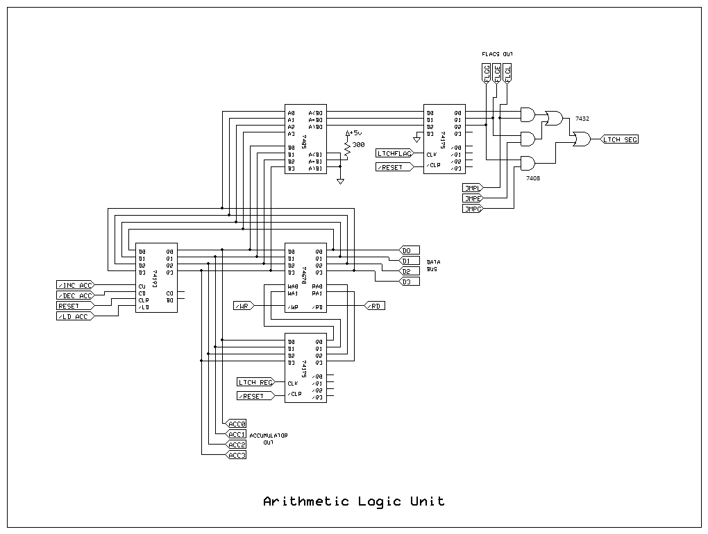
This is the arithmetic logic unit of the CPU. It doesn't do a whole lot of arithmetic. The accumulator can be incremented and decremented. Also, the accumulator can be compared to one of the registers or a literal value in the program code.
An instruction is composed of a four bit instruction code and optional four bits of program data. This program data can be loaded into the accumulator or may be compared to the accumulator. Data cannot be written back to program memory at runtime.
The accumulator -
The accumulator is a 74LS193 which is a four bit, up-down counter that can be loaded with data. Any data loaded from program memory or from input passes through the accumulator first. Also, the four registers are read from and written to by the accumulator. When the accumulator is loaded, the source of data is enabled on the data bus (they are all tri-state devices) for three clock cycles. The accumulator is loaded on the second (middle) clock cycle. This is done to ensure the inputs at the 74LS193 are stable when the data is loaded.
The registers -
The registers are implemented with a 74LS670, which is similar to the 74LS170 but has tri-state outputs. This is a 4x4 register file (four, 4 bit words). The address of the individual registers are held in a 74LS175 four bit latch. The contents of the register address latch are written to by the accumulator with the REG instruction. The input and output addresses are independent of each other. When a register is read, the register output is activated on the data bus while the accumulator is loaded. The register addresses are formated as follows -
        Four bit word : RRWW

        WW - Write address.
        RR - Read address.

	00 - Register A
	01 - Register B
	10 - Register C
	11 - Register D
Comparing the accumulator and flags -
The accumulator can be compared to a literal value in program memory or a register. When a literal value is compared, the program data memory (2114) is activated on the data bus for three clock cycles while the flags latch is set. Likewise, to compare the accumulator to a register, the register is activated on the data bus for three clock cycles while the flags latch is set.
A 74LS85, a four bit magnitude comparator is used for making the comparison. It has three outputs, less than, equal and greater than. This gives us three flags. The output of the 74LS85 is latched in a 74LS175 latch when a CMPL or CMPR instruction is executed. A group of AND and OR gates are used to execute a jump when a given flag is set. The LTCH SEG output of the last OR gate will load the program address segment latch with the accumulator contents when it goes high. The JMPL, JMPE and JMPG connections to the AND gates determine which flag to check for a jump. If the flag is set, the segement register is loaded causing program execution to jump to another program segement.
Connections to other schematics -
Here is a listing of the connections to other schematics.
| RESET | Active high reset. |
|---|---|
| /RESET | Active low reset. |
| INS0 through INS3 | Instruction code from program memory. |
| LTCHFLAG | Active high signal to latch the flags into the flags register. |
| /WR | Active low signal to write the accumulator to a register. |
| LTCH REG | Active high signal to latch the register address into the register address latch. |
| /DEC ACC | Active low signal to decrement the accumulator. |
| /INC ACC | Active low signal to increment the accumulator. |
| /LD ACC | Active low signal to load the accumulator. |
| INC PC | Active high signal to increment the program counter. |
| LTCH INS | Active high signal to latch the program instruction into the instruction latch. |
| /E INPUT | Active low signal to enable input lines on the data bus. |
| /E INS DATA | Active low signal to enable program data on the data bus. |
| /RD | Active low signal to enable the selected register on the data bus. |
| OUT LTCH | Active high signal to latch the accumulator into the output latch. |
| /RESTART | Active low signal to reset the program counter. |
| JMPG | Active high signal to latch the segment register when the greater than flag is set. |
| JMPE | Active high signal to latch the segment register when the equal flag is set. |
| JMPL | Active high signal to latch the segment register when the less than flag is set. |

The program memory is stored in 2114 static RAMs and is addressed by a program counter and a segment register. The memory address is latched during the fetch cycle and held during instruction execution. Latching the memory address is necessary because the program counter and segment register may change when the instruction is executed (during a RESTART or JUMP instructions). The new values in the program counter and segment register (if any) will be effective during the next fetch cycle.
Addressing -
The program counter is a 74LS161 four bit counter. The loading functionality of the 74LS161 is not used here, but the reset (clear) input on the 74LS161 is active low, which is desireable in this case. During program execution, the program counter is incremented for each instruction and supplies the four least significant bits of the memory address. The program counter may be reset during a reset of the CPU or by the RESTART instruction. The program counter is also reset when the segment register is changed. The AND gate on the clear input of the 74LS161 allows both the CPU reset and RESTART instruction to reset the program counter.
The segment register is a 74LS175 four bit latch. This supplies the four most significant bits of the memory address. The segment register is loaded from the accumulator during a JUMPL, JUMPE or JIMPG instruction if the appropriate flag is set.
The memory address is latched in a 74LS374 eight bit latch. The address is held in the latch during instruction execution and is updated during the fetch cycle. The outputs of the 74LS374 are tri-state and are put into high impedence mode when the memory is being loaded with a program.
Memory -
Program memory is stored in two, 2114 static RAMs. 2112s could have been used as well. Since only an eight bit address is used, a program is limited to 256 instructions. The address is supplied by the 74LS374 address latch during program run time and from the programmer interface during programming. The instruction data RAM is connected to the data bus where it can be loaded into the accumulator. The instruction code RAM is connected to the micro-instruction circutry and is used as an offset for loading the micro-instruction code. AND gates are used to generate the proper select and write signals for the 2114s. a /PRG WRITE signal from the programming interface both selects the memory and writes to it. The outputs on the 2114 are tri-state and in high impedence mode when not selected. During program run time, the program instruction RAM is always selected (read mode) while the program data RAM is selected to read only to load the accumulator with a literal value or when comparing the accumulator to a literal value.
Connections to other schematics -
Here is a listing of the connections to other schematics.
| /RESET | Active low reset. |
|---|---|
| INC PC | Active high signal to increment the program counter (from EPROM). |
| /RESTART | Active low signal to reset the program counter (from EPROM). |
| LTCH SEG | Active high signal to latch the segment address into the segment register (from ALU). |
| LTCH INS | Active high signal to latch the program instruction into the instruction latch (from EPROM). |
| /E INS DATA | Active low signal to enable program data on the data bus (from EPROM). |
| /RUN MODE | Active low signal to enable address latch on address bus (from control / programming interface). |
| /PRG WRITE | Active low signal to to write to program memory (from control / programming interface). |
| INS0 through INS3 | Instruction code from program memory. Also connected to programming interface. |
| D0 through D3 | Data bus to accumulator. Also connected to programming interface. |
| ACC0 through ACC3 | From accumulator. |
| ADR0 through ADR7 | Memory address from programming interface. |

The I/O circuitry is fairly simple. The output data is latched in a 74LS175 four bit latch and pushed through half of a 74LS244 buffer. Likewise the input comes in through the other half of the 74LS244 buffer. When reading from input, the input is made active on the data bus for three clock cycles while the accumulator is loaded. Monitoring of the input and output is done with a second 74LS244, which is used as a driver for the LEDs.
Connections to other schematics -
Here is a listing of the connections to other schematics.
| /RESET | Active low reset. |
|---|---|
| /E INPUT | Active low signal to enable input lines on the data buss. |
| OUT LTCH | Active high signal to latch the accumulator into the output latch. |
| D0 through D3 | Data bus to accumulator. |
| IN0 through IN3 | Inputs from the outside world. |
| OUT0 through OUT3 | Outputs to the outside world. |

The programming interface is a simple toggle switch / LED type. Since programs written for this 4 bit CPU are relatively simple and small, the toggle switch /LED interface works well and is not as difficult to use as one may think.
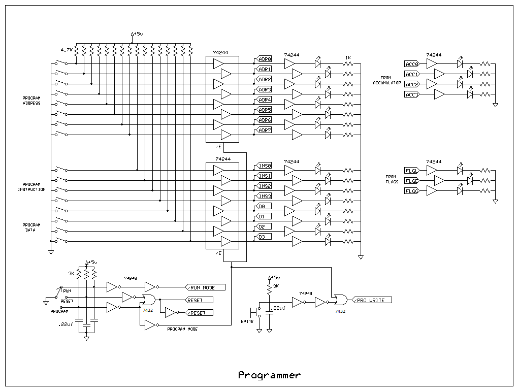
Programmer -
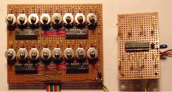
The toggle swithes are connected to 74LS244 buffers. The buffers are in high impedence state at program run time and reset mode and are active during programming mode. The memory address, instruction and program data are input through the toggle switches. There are another set of 74LS244 buffers used to drive the LEDs. These show the memory address, instruction and program data both during programming and program run time.
The contents of the accumulator and flags register are also displayed during runtime through 74LS244 buffers at program run time. This is useful when testing and debugging programs. The lowest clock speed (10 Hz) is necessary to observe the accumulator and flags during program testing.
Control -
There are three modes of operation : run, reset and program. A program may be loaded into memory when in program mode and of course the program run in run mode. Reset mode holds the entire CPU in reset. Reset mode is the center position in the three way rotary switch so that the only transition from run mode or program mode is through reset. The CPU is in reset mode during programming mode as well. The address and instruction LEDs will glow in reset mode because everything in the CPU is in high impedence state at this time.
There is a write button to write an instruction and data to memory while in program mode. WRITE switch is automatically activated during PROGRAM mode only, to avoid accidentally writing to memory during program execution.
A 74LS240 is used for switch de-bouncing. Although the 74LS240, '241 and '244 are buffers, they are also Schmidt triggers and work well for de-bouncing switches and buttons.
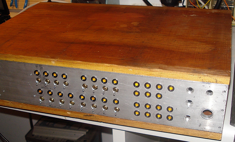
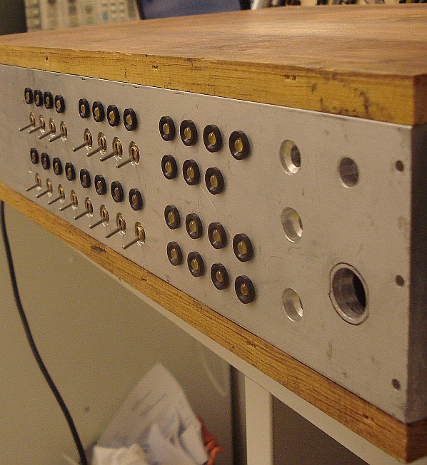
Construction notes -
The control panel is made from 3/32" aluminum sheet. This material is easy to cut and drill with hand tools. The aluminum sheet was purchased from a local hardware store.
The control panel shows controls and LEDs not used in this 4 bit CPU for they were installed for an earlier and abortive version of the CPU. These are the zero flag indicator, step button and step / cont switch. The button and switch were meant for a single instruction execution mode that was deleted from the final version of the CPU to reduce complexity, as was the zero flag.
The power switch and pilot light are also not functional. I haven't yet built a power supply for the CPU and I currently run it from an external power supply.
One of the pictures shows the toggle switch board and flags / accumulator display board. The toggle swithes are installed on a board along with the 74LS244 buffers and LEDs. The LEDs were soldered in only after the switches were attached by nuts to the panel and the LEDs they were positioned in their holes in the panel. This ensured the proper distance from the LED and board. The same technique was used for the flags / accumulator displays after the board was attached to the stand-offs.
The connectors to the CPU board are DIP headers. An 8 header is used for the control interface and a 16 pin header is used for the address and instruction interface. These headers connect to the empty sockets on the CPU board.
These are sample programs that don't do much more than push data to the output. These are not practical useful applications and only serve to demonstrate and exercise the CPU.
The first program simply loads a value from a register, increments it, outputs the value and writes the value back to the register. The process is repeated continually. The output is connected to 4 LEDs.
Numonic   Address    Data Instruction   Comments
------------------------------------------------------------------------------------------
                                        Runs in segement zero.
LIT 1     0000 0000  0001 0000          Put 0 in the accumulator.
REG       0000 0001  0000 0110          Select register A.
LOAD      0000 0010  0000 0010          Load value into accumulator from register A.
OUT       0000 0011  0000 1110          Send accumulator value to output.
INC       0000 0100  0000 0100          Increment accumulator.
STORE     0000 0101  0000 0011          Store accumulator back to register A.
RST       0000 0110  0000 1001          Restart program counter.
This program stores a sequence of values in the registers and then outputs them in sequence. The resulting effect is the output lines going high in a 1, 2, 4, 8 order. The program continuously loops from segments 2 to 3. This can be seen when LEDs are connected to the outputs.
Numonic   Address    Data Instruction   Comments
------------------------------------------------------------------------------------------
                                        Runs in 4 memory segments.
                                        Segment 0. Loads registers A and B.
LIT 0     0000 0000  0000 0001          Put 0 in the accumulator.
REG       0000 0001  0000 0110          Select register A for write.
LIT 1     0000 0010  0001 0001          Put 1 in the accumulator.
STORE     0000 0011  0000 0011          Put 1 in register A.
LIT 1     0000 0100  0001 0001          Put 1 again in the accumulator.
REG       0000 0101  0000 0110          Select register B for write.
LIT 2     0000 0110  0010 0001          Put 2 in the accumulator.
STORE     0000 0111  0000 0011          Put 2 in register B.
CMPL      0000 1000  0010 0111          Compare to last accumulator value. Set equal flag.
LIT 1     0000 1001  0001 0001          Put 1 in the accumulator.
JUMPE     0000 1010  0000 1011          Jump to segment 1.
                                        Segment 1. Loads registers C and D.
LIT 2     0001 0000  0010 0001          Put 2 in the accumulator.
REG       0001 0001  0000 0110          Select register C for write.
LIT 4     0001 0100  0100 0001          Put 4 in the accumulator.
STORE     0001 0011  0000 0011          Put 4 in register C.
LIT 3     0001 0100  0011 0001          Put 3 in the accumulator.
REG       0001 0101  0000 0110          Select register D for write.
LIT 8     0001 0110  1000 0001          Put 8 in the accumulator.
STORE     0001 0111  0000 0011          Put 8 in register D.
CMPL      0001 1000  1000 0111          Compare to last accumulator value. Set equal flag.
LIT 2     0001 1001  0010 0001          Put 2 in the accumulator.
JUMPE     0001 1010  0000 1011          Jump to segment 2.
                                        Segment 2. Sends registers A and B to output.
LIT 0     0010 0000  0000 0001          Put 0 in the accumulator.
REG       0010 0001  0000 0110          Select register A for read.
LOAD      0010 0010  0000 0010          Load register A to accumulator.
OUT       0010 0011  0000 1110          Output accumulator (register A).
LIT 4     0010 0100  0100 0001          Put 4 in the accumulator.
REG       0010 0101  0000 0110          Select register B for read.
LOAD      0010 0110  0000 1010          Load register B to accumulator.
OUT       0010 0111  0000 1110          Output accumulator (register B).
CMPR      0010 1000  0000 1000          Compare accumulator to register. Set equal flag.
LIT 3     0010 1001  0011 0001          Put 3 in the accumulator.
JUMPE     0010 1010  0000 1110          Jump to segment 3.
                                        Segment 3. Sends registers C and D to output.
LIT 8     0011 0000  1000 0001          Put 8 in the accumulator.
REG       0011 0001  0000 0110          Select register C for read.
LOAD      0011 0010  0000 0010          Load register C to accumulator.
OUT       0011 0011  0000 1110          Output accumulator (register C).
LIT 12    0011 0100  1100 0001          Put 12 in the accumulator.
REG       0011 0101  0000 0110          Select register D for read.
LOAD      0011 0110  0000 1010          Load register D to accumulator.
OUT       0011 0111  0000 1110          Output accumulator (register D).
CMPR      0011 1000  0000 1000          Compare accumulator to register. Set equal flag.
LIT 3     0011 1001  0010 0001          Put 2 in the accumulator.
JUMPE     0011 1010  0000 1110          Jump to back to segment 2 - loop.
The enclosure for the computer can be made from thick aluminum front and back plates and a few solid cherry tree wood plates for the rest of it's parts. These materials were thought to be very stable mechanically and at the same time highlight the vintage character of the project. A few preliminary photos of how the enclosure has been thought to be made, are shown below.
Later on, markings will be stamped on the front panel using a letter punch kit, to denote the functions of the switches and the LEDs.
The address, data and instruction switches, as well as the LEDs, have been placed on the front panel in a aligned and symmetrical way.
To be continued...
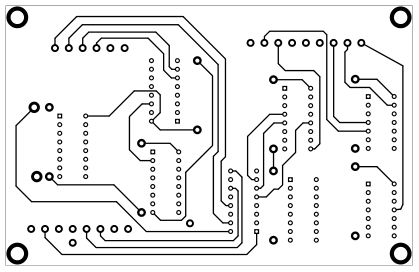
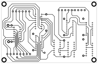
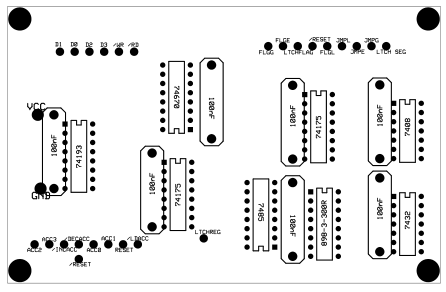
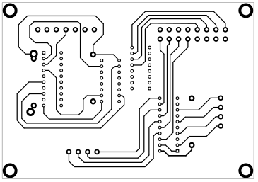
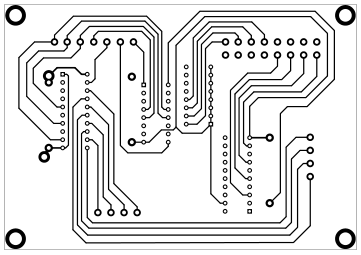
Here are the PCBs I have designed for the computer so far. Click on the links or the images, to download the files for etching.
Programming interface
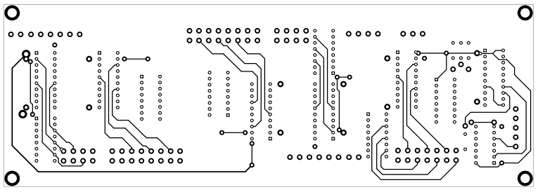
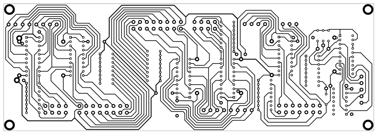
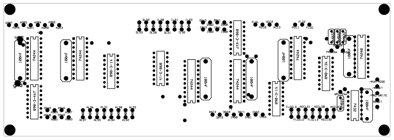
Arithmetic logic unit
Input / output
A possible problem when building this project, is the code that needs to be written into the EPROMs. A suitable programmer and a personal computer is needed to program them. An alternative solution, that does not need a personal computer, is the manual EPROM programmer shown here. The programming is done step-by-step using a series of switches, to select the address of the EPROM to be programmed and the data that needs to be written to that address.
To program each of the two EPROMs, refer to the Micro-instruction Code Detail section. Starting from address zero and incrementing by one address each time, set the relevant eight data bits for each of the two EPROMs. As it is shown on the clock/micro-instruction schematic, D0 of the first EPROM is the LTCH FLAG and D7 of this EPROM is the LTCH INS. Similarly, D0 of the second EPROM is the /E IN and D7 of this EPROM is the JMPL.

Schematic and information of the 2716 manual EPROM programmer (PDF)