Inside Computer Logic
Gates
Original article by
Ken Bigelow and
some more additions
Just what goes on inside logic gates to actually perform logic functions? Here are the internal schematics of various gates, as implemented by several different logic families.
I won't cover the internal operation of individual semiconductor devices in these pages, except to state the basic behavior of a given device under specific conditions. More detailed coverage of semiconductor physics and internal behavior is a job for another set of pages.
There are several different families of logic gates. Each family has its capabilities and limitations, its advantages and disadvantages. The following list describes the main logic families and their characteristics. You can follow the links to see the circuit construction of gates of each family.
Relay logic (RL)
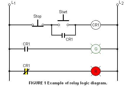
The schematic diagrams for relay logic circuits are often called line diagrams, because the inputs and outputs are essentially drawn in a series of lines. A relay logic circuit is an electrical network consisting of lines, or rungs, in which each line or rung must have continuity to enable the output device. A typical circuit consists of a number of rungs, with each rung controlling an output. This output is controlled by a combination of input or output conditions, such as input switches and control relays. The conditions that represent the inputs are connected in series, parallel, or series-parallel to obtain the logic required to drive the output. The relay logic circuit forms an electrical schematic diagram for the control of input and output devices. Relay logic diagrams represent the physical interconnection of devices. The basic format for relay logic diagrams is as follows:
1. The two vertical lines that connect all devices on the relay logic diagram are labeled L1 and L2. The space between L1 and L2 represents the voltage of the control circuit.
2. Output devices are always connected to L2. Any electrical overloads that are to be included must be shown between the output device and L2; otherwise, the output device must be the last component before L2.
3. Control devices are always shown between L1 and the output device. Control devices may be connected either in series or in parallel with each other.
4. Devices which perform a STOP function are usually connected in series, while devices that perform a START function are connected in parallel.
5. Electrical devices are shown in their normal conditions. An NC contact would be shown as normally closed, and an NO contact would appear as a normally open device. All contacts associated with a device will change state when the device is energized.
Figure below shows a typical relay logic diagram. In this circuit, a STOP/START station is used to control two pilot lights. When the START button is pressed, the control relay energizes and its associated contacts change state. The green pilot light is now ON and the red lamp is OFF. When the STOP button is pressed, the contacts return to their resting state, the red pilot light is ON, and the green switches OFF.
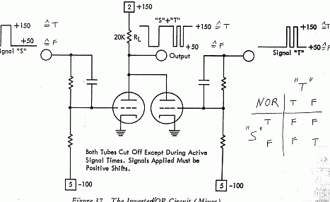
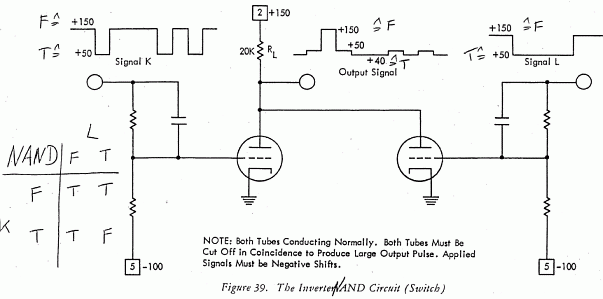
VTL is a term that I have given to describe the logic circuits that use vacuum tubes. I do not know if this was called like this back then. There is an analytical explanation of gates created using vacuum tubes in this article and this one too (pdf).
Here are two examples of gates that can be constructed using vacuum tubes. As you would expect, the voltage levels are high and also much power is consumed to keep the tube filaments hot.
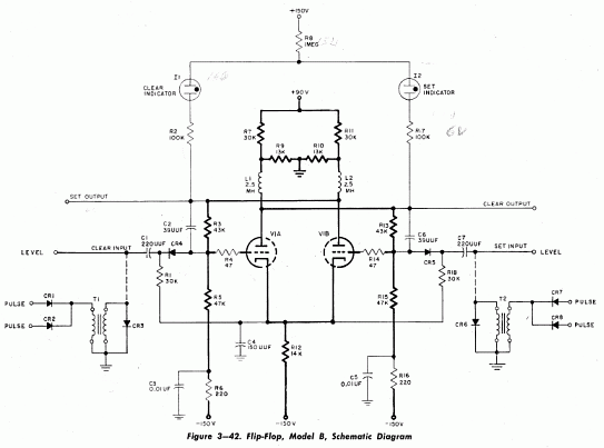
DVTL is a term that I have given to describe the logic circuits that use vacuum tube gates in combination with diode gates. I do not know if this was called like this back then.
By letting diodes perform the logical AND or OR function and then amplifying the result with a vacuum tube, we can reduce cost significantly. DVTL takes diode logic gates and adds a vacuum tube to the output, in order to provide logic inversion and to restore the signal to full logic levels.
Here is an example of a combination of a tube circuit and diode gates to form a flip-flop, not a true tube gate but just for illustration. Again refer to this article for a more analytical explanation.
Diode Logic (DL)
Diode logic gates are very simple and inexpensive, and can be used effectively in specific situations. However, they cannot be used extensively, as they tend to degrade digital signals rapidly. In addition, they cannot perform a NOT function, so their usefulness is quite limited.
Diode Logic makes use of the fact that the electronic device known as a diode will conduct an electrical current in one direction, but not in the other. In this manner, the diode acts as an electronic switch.
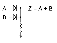
To the left you see a basic Diode Logic OR gate. We'll assume that a logic 1 is represented by +5 volts, and a logic 0 is represented by ground, or zero volts. In this figure, if both inputs are left unconnected or are both at logic 0, output Z will also be held at zero volts by the resistor, and will thus be a logic 0 as well. However, if either input is raised to +5 volts, its diode will become forward biased and will therefore conduct. This in turn will force the output up to logic 1. If both inputs are logic 1, the output will still be logic 1. Hence, this gate correctly performs a logical OR function.
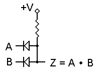
To the right is the equivalent AND gate. We use the same logic levels, but the diodes are reversed and the resistor is set to pull the output voltage up to a logic 1 state. For this example, +V = +5 volts, although other voltages can just as easily be used. Now, if both inputs are unconnected or if they are both at logic 1, output Z will be at logic 1. If either input is grounded (logic 0), that diode will conduct and will pull the output down to logic 0 as well. Both inputs must be logic 1 in order for the output to be logic 1, so this circuit performs the logical AND function.
In both of these gates, we have made the assumption that the diodes do not introduce any errors or losses into the circuit. This is not really the case; a silicon diode will experience a forward voltage drop of about 0.65v to 0.7v while conducting. But we can get around this very nicely by specifying that any voltage above +3.5 volts shall be logic 1, and any voltage below +1.5 volts shall be logic 0. It is illegal in this system for an output voltage to be between +1.5 and +3.5 volts; this is the undefined voltage region.
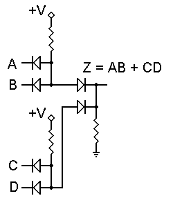
Individual gates like the two above can be used to advantage in specific circumstances. However, when DL gates are cascaded, as shown to the left, some additional problems occur. Here, we have two AND gates, whose outputs are connected to the inputs of an OR gate. Very simple and apparently reasonable.
But wait a minute! If we pull the inputs down to logic 0, sure enough the output will be held at logic 0. However, if both inputs of either AND gate are at +5 volts, what will the output voltage be? That diode in the OR gate will immediately be forward biased, and current will flow through the AND gate resistor, through the diode, and through the OR gate resistor.
If we assume that all resistors are of equal value (typically, they are), they will act as a voltage divider and equally share the +5 volt supply voltage. The OR gate diode will insert its small loss into the system, and the output voltage will be about 2.1 to 2.2 volts. If both AND gates have logic 1 inputs, the output voltage can rise to about 2.8 to 2.9 volts. Clearly, this is in the "forbidden zone," which is not supposed to be permitted.
If we go one step further and connect the outputs of two or more of these structures to another AND gate, we will have lost all control over the output voltage; there will always be a reverse-biased diode somewhere blocking the input signals and preventing the circuit from operating correctly. This is why Diode Logic is used only for single gates, and only in specific circumstances
GDTL is a term that I have given to describe the logic circuits that use cold cathode gas discharge tube gates. I do not know if this was called like this back then. More analytical information about logic circuits using gas discharge tubes can be found in this article (pdf).
Two examples of logic gates are shown below.
Resistor-Transistor Logic (RTL)
RTL gates are almost as simple as DL gates, and remain inexpensive. They also are handy because both normal and inverted signals are often available. However, they do draw a significant amount of current from the power supply for each gate. Another limitation is that RTL gates cannot switch at the high speeds used by today's computers, although they are still useful in slower applications.
Although they are not designed for linear operation, RTL integrated circuits are sometimes used as inexpensive small-signal amplifiers, or as interface devices between linear and digital circuits.
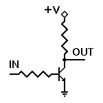
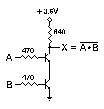
Consider the most basic transistor circuit, such as the one shown to the
left. We will only be applying one of two voltages to the input I: 0 volts
(logic 0) or +V volts (logic 1). The exact voltage used as +V depends on the
circuit design parameters; in RTL integrated circuits, the usual voltage is
+3.6v. We'll assume an ordinary NPN transistor here, with a reasonable dc
current gain, an emitter-base forward voltage of 0.65 volt, and a
collector-emitter saturation voltage no higher than 0.3 volt. In standard RTL
ICs, the base resistor is 470![]() and the collector resistor is 640
and the collector resistor is 640![]() .
.
When the input voltage is zero volts (actually, anything under 0.5 volt), there is no forward bias to the emitter-base junction, and the transistor does not conduct. Therefore no current flows through the collector resistor, and the output voltage is +V volts. Hence, a logic 0 input results in a logic 1 output.
When the input voltage is +V volts, the transistor's emitter-base junction
will clearly be forward biased. For those who like the mathematics, we'll assume
a similar output circuit connected to this input. Thus, we'll have a voltage of
3.6 - 0.65 = 2.95 volts applied across a series combination of a 640![]() output resistor and a 470
output resistor and a 470![]() input resistor. This gives us a base current of:
input resistor. This gives us a base current of:
RTL is a relatively old technology, and the transistors used in RTL ICs have a
dc forward current gain of around 30. If we assume a current gain of 30, 2.66 ma
base current will support a maximum of 79.8 ma collector current. However, if we
drop all but 0.3 volts across the 640![]() collector resistor, it will carry 3.3/640
collector resistor, it will carry 3.3/640![]() = 5.1 ma. Therefore this transistor is indeed fully saturated; it is turned on
as hard as it can be.
= 5.1 ma. Therefore this transistor is indeed fully saturated; it is turned on
as hard as it can be.
With a logic 1 input, then, this circuit produces a logic 0 output. We have already seen that a logic 0 input will produce a logic 1 output. Hence, this is a basic inverter circuit.
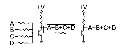
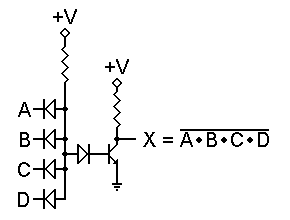
As we can see from the above calculations, the amount of current provided to the base of the transistor is far more than is necessary to drive the transistor into saturation. Therefore, we have the possibility of using one output to drive multiple inputs of other gates, and of having gates with multiple input resistors. Such a circuit is shown to the right.
In this circuit, we have four input resistors. Raising any one input to +3.6
volts will be sufficient to turn the transistor on, and applying additional
logic 1 (+3.6 volt) inputs will not really have any appreciable effect on the
output voltage. Remember that the forward bias voltage on the transistor's base
will not exceed 0.65 volt, so the current through a grounded input resistor will
not exceed 0.65v/470![]() = 1.383 ma. This does provide us with a practical limit on the number of
allowable input resistors to a single transistor, but doesn't cause any serious
problems within that limit.
= 1.383 ma. This does provide us with a practical limit on the number of
allowable input resistors to a single transistor, but doesn't cause any serious
problems within that limit.
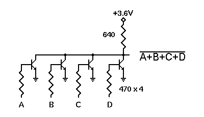
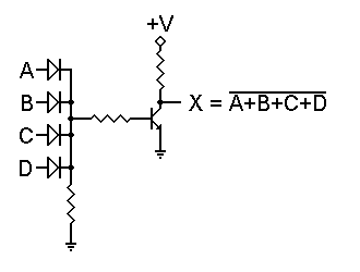
The RTL gate shown above will work, but has a problem due to possible signal interactions through the multiple input resistors. A better way to implement the NOR function is shown to the left.
Here, each transistor has only one input resistor, so there is no interaction between inputs. The NOR function is performed at the common collector connection of all transistors, which share a single collector load resistor.
This is in fact the pattern for all standard RTL ICs. The very commonly-used µL914 is a dual two-input NOR gate, where each gate is a two-transistor version of the circuit to the left. It is rated to draw 12 ma of current from the 3.6V power supply when both outputs are at logic 0. This corresponds quite well with the calculations we have already made.
Standard fan-out for RTL gates is rated at 16. However, the fan-in for a standard RTL gate input is 3. Thus, a gate can produce 16 units of drive current from the output, but requires 3 units to drive an input. There are low-power versions of these gates that increase the values of the base and collector resistors to 1.5K and 3.6K, respectively. Such gates demand less current, and typically have a fan-in of 1 and a fan-out of 2 or 3. They also have reduced frequency response, so they cannot operate as rapidly as the standard gates. To get greater output drive capabilities, buffers are used. These are typically inverters which have been designed with a fan-out of 80. They also have a fan-in requirement of 6, since they use pairs of input transistors to get increased drive.
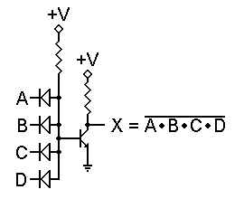
We can get a NAND function in either of two ways. We can simply invert the inputs to the NOR/OR gate, thus turning it into an AND/NAND gate, or we can use the circuit shown to the right.
In this circuit, each transistor has its own separate input resistor, so each is controlled by a different input signal. However, the only way the output can be pulled down to logic 0 is if both transistors are turned on by logic 1 inputs. If either input is a logic 0 that transistor cannot conduct, so there is no current through either one. The output is then a logic 1. This is the behavior of a NAND gate. Of course, an inverter can also be included to provide an AND output at the same time.
The problem with this NAND circuit stems from the fact that transistors are not ideal devices. Remember that 0.3 volt collector saturation voltage? Ideally it should be zero. Since it isn't, we need to look at what happens when we "stack" transistors this way. With two, the combined collector saturation voltage is 0.6 volt -- only slightly less than the 0.65 volt base voltage that will turn a transistor on.
If we stack three transistors for a 3-input NAND gate, the combined collector saturation voltage is 0.9 volt. This is too high; it will promote conduction in the next transistor no matter what. In addition, the load presented by the upper transistor to the gate that drives it will be different from the load presented by the lower transistor. This kind of unevenness can cause some odd problems to appear, especially as the frequency of operation increases. Because of these problems, this approach is not used in standard RTL ICs.
Diode-Transistor Logic (DTL)
As we said in the page on diode logic, the basic problem with DL gates is that they rapidly deteriorate the logical signal. However, they do work for one stage at a time, if the signal is re-amplified between gates. Diode-Transistor Logic (DTL) accomplishes that goal.
The gate to the right is a DL OR gate followed by an inverter. The OR function is still performed by the diodes. However, regardless of the number of logic 1 inputs, there is certain to be a high enough input voltage to drive the transistor into saturation. Only if all inputs are logic 0 will the transistor be held off. Thus, this circuit performs a NOR function.
The advantage of this circuit over its RTL equivalent is that the OR logic is performed by the diodes, not by resistors. Therefore there is no interaction between different inputs, and any number of diodes may be used. A disadvantage of this circuit is the input resistor to the transistor. Its presence tends to slow the circuit down, thus limiting the speed at which the transistor is able to switch states.
At first glance, the NAND version shown on the left should eliminate this problem. Any logic 0 input will immediately pull the transistor base down and turn the transistor off, right?
Well, not quite. Remember that 0.65 volt base input voltage for the transistor? Diodes exhibit a very similar forward voltage when they're conducting current. Therefore, even with all inputs at ground, the transistor's base will be at about 0.65 volt, and the transistor can conduct.
To solve this problem, we can add a diode in series with the transistor's base lead, as shown to the right. Now the forward voltage needed to turn the transistor on is 1.3 volts. For even more insurance, we could add a second series diode and require 1.95 volts to turn the transistor on. That way we can also be sure that temperature changes won't significantly affect the operation of the circuit.
Either way, this circuit will work as a NAND gate. In addition, as with the NOR gate, we can use as many input diodes as we may wish without raising the voltage threshold. Furthermore, with no series resistor in the input circuit, there is less of a slowdown effect, so the gate can switch states more rapidly and handle higher frequencies. The next obvious question is, can we rearrange things so the NOR gate can avoid that resistor, and therefore switch faster as well?
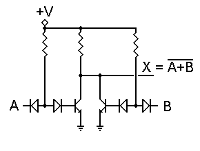
The answer is, Yes, there is. Consider the circuit shown to the left. Here we use separate transistors connected together. Each has a single input, and therefore functions as an inverter by itself. However, with the transistor collectors connected together, a logic 1 applied to either input will force the output to logic 0. This is the NOR function.
We can use multiple input diodes on either or both transistors, as with the DTL NAND gate. This would give us an AND-NOR function, and is useful in some circumstances. Such a construction is also known as an AOI (for AND-OR-INVERT) circuit.
Transistor-Transistor Logic (TTL)
As the state of the art improved, TTL integrated circuits were adapted slightly to handle a wider range of requirements, but their basic functions remained the same. These devices comprise the 7400 family of digital ICs.
With the rapid development of integrated circuits (ICs), new problems were encountered and new solutions were developed. One of the problems with DTL circuits was that it takes as much room on the IC chip to construct a diode as it does to construct a transistor. Since "real estate" is exceedingly important in ICs, it was desirable to find a way to avoid requiring large numbers of input diodes. But what could be used to replace many diodes?
Well, looking at the DTL NAND gate to the right, we might note that the opposed diodes look pretty much like the two junctions of a transistor. In fact, if we were to have an inverter, it would have a single input diode, and we just might be able to replace the two opposed diodes with an NPN transistor to do the same job.
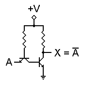
In fact, this works quite nicely. The figure to the left shows the resulting inverter.
In addition, we can add multiple emitters to the input transistor without greatly increasing the amount of space needed on the chip. This allows us to construct a multiple-input gate in almost the same space as an inverter. The resulting savings in real estate translates to a significant savings in manufacturing costs, which in turn reduces the cost to the end user of the device.
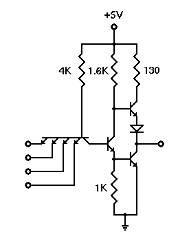
One problem shared by all logic gates with a single output transistor and a pull-up collector resistor is switching speed. The transistor actively pulls the output down to logic 0, but the resistor is not active in pulling the output up to logic 1. Due to inevitable factors such as circuit capacitances and a characteristic of bipolar transistors called "charge storage," it will take a certain amount of time for the transistor to turn completely off and the output to rise to a logic 1 level. This limits the frequency at which the gate can operate.
The designers of commercial TTL IC gates reduced that problem by modifying the output circuit. The result was the "totem pole" output circuit used in most of the 7400/5400 series TTL ICs. The final circuit used in most standard commercial TTL ICs is shown to the right. The number of inputs may vary — a commercial IC package might have six inverters, four 2-input gates, three 3-input gates, or two 4-input gates. An 8-input gate in one package is also available. But in each case, the circuit structure remains the same.
Emitter-Coupled Logic (ECL)
Emitter-Coupled Logic is based on the use of a multi-input differential amplifier to amplify and combine the digital signals, and emitter followers to adjust the dc voltage levels. As a result, none of the transistors in the gate ever enter saturation, nor do they ever get turned completely off. The transistors remain entirely within their active operating regions at all times. As a result, the transistors do not have a charge storage time to contend with, and can change states much more rapidly. Thus, the main advantage of this type of logic gate is extremely high speed.
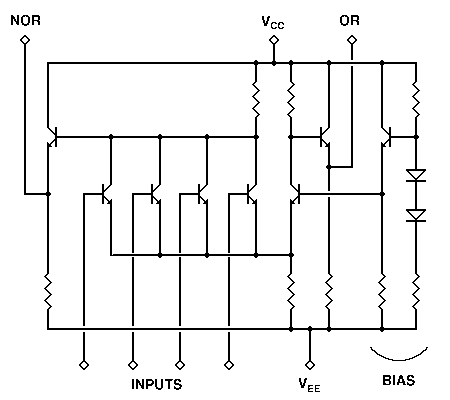
The schematic diagram shown here is taken from Motorola's 1000/10,000 series of MECL devices. This particular circuit is of one 4-input OR/NOR gate. Standard voltages for this circuit are -5.2 volts (VEE) and ground (VCC). Unused inputs are connected to VEE. The bias circuit at the right side, consisting of one transistor and its associated diodes and resistors, can handle any number of gates in a single IC package. Typical ICs include dual 4-input, triple 3-input, and quad 2-input gates. In each case, the gates themselves differ only in how many input transistors they have. A single bias circuit serves all gates.
In operation, a logical ouput changes state by only 0.85 volt, from a low of -1.60 volts to a high of -0.75 volt. The internal bias circuit supplies a fixed voltage of -1.175 volts to the bias transistor in the differential amplifier. If all inputs are at -1.6 volts (or tied to VEE), the input transistors will all be off, and only the internal differential transistor will conduct current. This reduces the base voltage of the OR output transistor, lowering its output voltage to -1.60 volts. At the same time, no input transistors are affecting the NOR output transistor's base, so its output rises to -0.75 volt. This is simply the emitter-base voltage, VBE, of the transistor itself. (All transistors are alike within the IC, and are designed to have a VBE of 0.75 volt.)
When any input rises to -0.75 volt, that transistor siphons emitter current away from the internal differential transistor, causing the outputs to switch states.
The voltage changes in this type of circuit are small, and are dictated by the VBE of the transistors involved when they are on. Of greater importance to the operation of the circuit is the amount of current flowing through various transistors, rather than the precise voltages involved. Accordingly, Emitter-Coupled Logic is also known as Current Mode Logic (CML). This is not the only technology to implement CML by any means, but it does fall into that general description. In any case, this leads us to a major drawback of this type of gate: it draws a great deal of current from the power supply, and hence tends to dissipate a significant amount of heat.
To minimize this problem, some devices such as frequency counters use an ECL decade counter at the input end of the circuitry, followed by TTL or high-speed CMOS counters at the later digit positions. This puts the fast, expensive IC where it is absolutely required, and allows us to use cheaper ICs in locations where the signal will never be at that high a frequency.
CMOS Logic
CMOS gates are, however, severely limited in their speed of operation. Nevertheless, they are highly useful and effective in a wide range of battery-powered applications.
CMOS logic is a newer technology, based on the use of complementary MOS transistors to perform logic functions with almost no current required. This makes these gates very useful in battery-powered applications. The fact that they will work with supply voltages as low as 3 volts and as high as 15 volts is also very helpful.
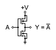
CMOS gates are all based on the fundamental inverter circuit shown to the left. Note that both transistors are enhancement-mode MOSFETs; one N-channel with its source grounded, and one P-channel with its source connected to +V. Their gates are connected together to form the input, and their drains are connected together to form the output.
The two MOSFETs are designed to have matching characteristics. Thus, they are
complementary to each other. When off, their resistance is effectively infinite;
when on, their channel resistance is about 200 ![]() .
Since the gate is essentially an open circuit it draws no current, and the
output voltage will be equal to either ground or to the power supply voltage,
depending on which transistor is conducting.
.
Since the gate is essentially an open circuit it draws no current, and the
output voltage will be equal to either ground or to the power supply voltage,
depending on which transistor is conducting.
When input A is grounded (logic 0), the N-channel MOSFET is unbiased, and
therefore has no channel enhanced within itself. It is an open circuit, and
therefore leaves the output line disconnected from ground. At the same time, the
P-channel MOSFET is forward biased, so it has a channel enhanced within itself.
This channel has a resistance of about 200 ![]() ,
connecting the output line to the +V supply. This pulls the output up to +V
(logic 1).
,
connecting the output line to the +V supply. This pulls the output up to +V
(logic 1).
When input A is at +V (logic 1), the P-channel MOSFET is off and the N-channel MOSFET is on, thus pulling the output down to ground (logic 0). Thus, this circuit correctly performs logic inversion, and at the same time provides active pull-up and pull-down, according to the output state.
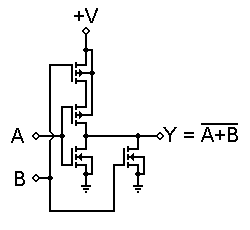
This concept can be expanded into NOR and NAND structures by combining inverters in a partially series, partially parallel structure. The circuit to the right is a practical example of a CMOS 2-input NOR gate.
In this circuit, if both inputs are low, both P-channel MOSFETs will be turned on, thus providing a connection to +V. Both N-channel MOSFETs will be off, so there will be no ground connection. However, if either input goes high, that P-channel MOSFET will turn off and disconnect the output from +V, while that N-channel MOSFET will turn on, thus grounding the output.
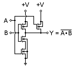
The structure can be inverted, as shown to the left. Here we have a two-input NAND gate, where a logic 0 at either input will force the output to logic 1, but it takes both inputs at logic 1 to allow the output to go to logic 0.
This structure is less limited than the bipolar equivalent would be, but there are still some practical limits. One of these is the combined resistance of the MOSFETs in series. As a result, CMOS totem poles are not made more than four inputs high. Gates with more than four inputs are built as cascading structures rather than single structures. However, the logic is still valid.
Even with this limit, the totem pole structure still causes some problems in certain applications. The pull-up and pull-down resistances at the output are never the same, and can change significantly as the inputs change state, even if the output does not change logic states. The result is uneven and unpredictable rise and fall times for the output signal. This problem was addressed, and was solved with the buffered, or B-series CMOS gates.
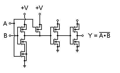
The technique here is to follow the actual NAND gate with a pair of inverters. Thus, the output will always be driven by a single transistor, either P-channel or N-channel. Since they are as closely matched as possible, the output resistance of the gate will always be the same, and signal behavior is therefore more predictable.
One of the main problems with CMOS gates is their speed. They cannot operate very quickly, because of their inherent input capacitance. B-series devices help to overcome these limitations to some extent, by providing uniform output current, and by switching output states more rapidly, even if the input signals are changing more slowly.
Note that we have not gone into all of the details of CMOS gate construction here. For example, to avoid damage caused by static electricity, different manufacturers developed a number of input protection circuits, to prevent input voltages from becoming too high. However, these protection circuits do not affect the logical behavior of the gates, so we will not go into the details here.
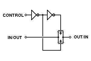
One type of gate, shown to the left, is unique to CMOS technology. This is the bilateral switch, or transmission gate. It makes full use of the fact that the individual FETs in a CMOS IC are constructed to be symmetrical. That is, the drain and source connections to any individual transistor can be interchanged without affecting the performance of either the transistor itself or the circuit as a whole.
When the N- and P-type FETs are connected as shown here and their gates are driven from complementary control signals, both transistors will be turned on or off together, rather than alternately. If they are both off, the signal path is essentially an open circuit — there is no connection between input and output. If they are both on, there is a very low-resistance connection between input and output, and a signal will be passed through.
What is truly interesting about this structure is that the signal being controlled in this manner does not have to be a digital signal. As long as the signal voltage does not exceed the power supply voltages, even an analog signal can be controlled by this type of gate.
Most logic families share a common characteristic: their inputs require a certain amount of current in order to operate correctly. CMOS gates work a bit differently, but still represent a capacitance that must be charged or discharged when the input changes state. The current required to drive any input must come from the output supplying the logic signal. Therefore, we need to know how much current an input requires, and how much current an output can reliably supply, in order to determine how many inputs may be connected to a single output.
However, making such calculations can be tedious, and can bog down logic circuit design. Therefore, we use a different technique. Rather than working constantly with actual currents, we determine the amount of current required to drive one standard input, and designate that as a standard load on any output. Now we can define the number of standard loads a given output can drive, and identify it that way. Unfortunately, some inputs for specialized circuits require more than the usual input current, and some gates, known as buffers, are deliberately designed to be able to drive more inputs than usual. For an easy way to define input current requirements and output drive capabilities, we define two new terms:
Fan-in
Fan-out
Remember, fan-in and fan-out apply directly only within a given logic family. If for any reason you need to interface between two different logic families, be careful to note and meet the drive requirements and limitations of both families, within the interface circuitry.