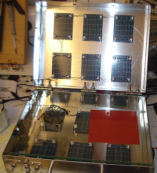
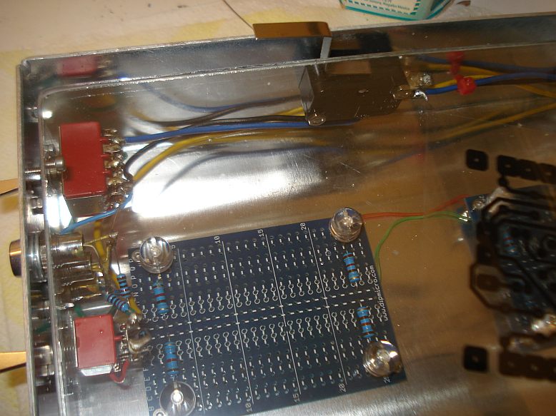
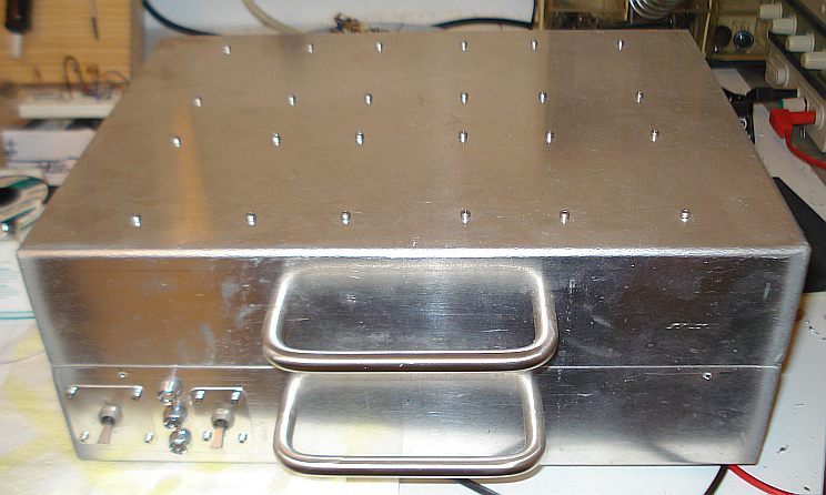
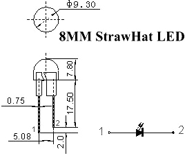
Solid state PCB exposure
by SV3ORA


After quite a lot of years of avoiding to make homemade PCBs, mainly due to the complexity and time required, I have finally decided that in some cases a PCB is needed. Thus, a PCB exposure box is very much needed in these cases, especially when dealing with high frequency projects. I had many projects which also required double sided PCBs, so I have decided to make a double sided PCB exposure box instead of manually flipping the PCB inside it. This exposure box used two 125W mercury vapour lamps, each 30cm above the PCB, which was sandwitched inside two glasses. This solution worked well but the enclosure was about 1m high. Apart from the lethal voltages, the two 125W lamps were also consumming a lot of power and they were producing a lot of heat. The need for a better and modern solution was born.

Technology has advanced very much the last decades and new solid state devices are out from time to time. With the new UV LEDs availability in extremely cheap prices, a solid state UV PCB exposure box seems a more efficient, cheaper, smaller and safer solution for the labratory, than ever.

The key point of making a good solid state UV PCB exposure box is the choice of the LEDs. LEDs usually exhibit high light directivity ranging from about 20 to 40 degrees @ 3dB. Whereas directivity is desired in some applications, it is not good for an exposure box. The solution most homebrewers choose is the use of many 100mW UV LEDs placed close together, so the light is spread almost evenly throughout the whole PCB. Others, use refraction sheets to refract the light, so that it is spread evenly throughout the PCB. Whereas these solutions work to some extent, they require a massive amount of leds and lots of soldering and labor to build. A better and easier to build solution exists, the "straw-hat" LED.

This type of LED, uses straw-hat shaped lens and it exhibits a much wider angle reaching up to about 140 degrees. However, as the spreading gets bigger, the radiated power per square cm degreases. This requires the use of more powerfull LEDs, to overcome this effective power loss. The LEDs used in the presented exposure box, are rated at 500mW, instead of the common UV ones which are typically 100mW. They have 5 LED dies inside the same package, instead of 1. By exhibiting a much wider angle and being more powerful, these LEDs can be placed further apart, so that fewer of them are required in total.

There are even more powerful LEDs to choose but all of them require external heatsinks to operate, which is more expensive and not so convenient in this application. The LEDs used, have overgrown internal cathodes, which are used as small internal heatsinks. Thus an external heatsink is not required, provided they are not overdriven. The picture below, shows such a LED in operation.


The viewing angle is much greater than that of the common LEDs. An angle of more than 90 degrees can be easily noticed. The technical specifications of the LEDs I have purchased, are shown in the tables below. With my purchase, the seller also provided a free current limiting resistor for each of the LEDs.

Specifications
  • Source Material:InGaN !
  • Emitting Colour:0.5W 8MM WIDE VIEW ULTRA VIOLET UV 400nm 0.5W LED 
  • LENS Type:Water clear
  • Color Temperature: --
  • Luminous Intensity-MCD: Typ: 30,000 mcd
  • Reverse Voltage:5.0 V
  • DC Forward Voltage: Typical:
  • DC Forward Current:100mA
  • Viewing Angle:140 degree
  • Lead Soldering Temp:260°C for 5 seconds

Absolute Maximum Rating (Ta = 250C)

PARAMETER

MAXIMUM RATING

UNITS

DC Forward Current

100

mA

Peak Pulse Forward Current (1)

150

mA

Avg. Forward Current (Pulse Operation)

100

mA

Operating Temperature

-40 to +100

0C

Storage Temperature

-40 to +120

0C

Lead Soldering Temperature

2600C for 6 seconds
(1.0mm or 0.63 inch from Body)

(1)  Pulse conditions of 1/10 duty and 0.1msec width 

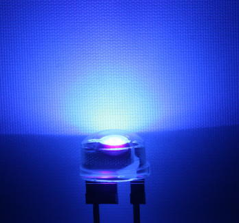
Electro-optical Characteristics (Ta = 250C)

PARAMETER

SYMBOL

CONDITIONS

MIN.

TYP.

MAX.

UNIT

Forward Voltage

VF

IF = 100mA

3.2

3.4

3.6

V

Reverse Voltage

VR

IR = 100mA

 -

 5

-

V

Dominant Wavelength

lD

IF = 100mA

395

400

405 

Viewing Angle

2q1/2

IF = 100mA


140


Deg.

Luminous Intensity

IV

IF = 100mA

-

 30,000

32,000

mcd


For the building of the exposure box, I have used two aluminium cooking pans to form the enclosure. Their size was about the size of an A4 sheet of paper. I have chosen this size based on the number of LEDs I had available, but also based on the maximum size of PCB I could find in local stores. The pans were purchased at low price from local stores.


I then used three stainless steel hinges (just two would probably be ok) to hold the pans in place so that they can be opened and closed together like a book. I mounted the LEDs and their current limiting resistors in 12 small prototype boards I had available and I mounted these boards into both pans, making sure that the LEDs are spaced almost equally apart. It is very important for The LEDs to be spaced equally apart, so that the UV light is evenly applied onto the exposed PCB.


Two A4-sized pieces of glass are placed inside the exposure box. The lower glass stants above the lower side of the LEDs using four side screws that are mounted onto the lower pan and extend inside it, to hold the glass in place. The upper glass just leans above the lower one. The PCB is placed between these two glasses during exposure. It is very important to mount the glasses in equal distance from each side of the LEDs, so that the PCB is exposed on its both sides by equal amount of UV light.

In the front pannel, there is an ON/OFF switch and another one (connected electrically in series with it) that enables either the upper LEDs only (for single sided PCB), or both the upper and the lower ones (for double sided PCB). There is also an ON/OFF LED indicator and LED indicators that show which LED side is enabled. These indicators may seem a bit optional, but it is good to include them, especially the ON/OFF one. Two stainless steel drawer handles have been also placed in the front panel, one at each pan. This allows more convenient opening and closing of the pans, but also minimizes the risk of accidentally moving out of place the exposed PCB inside the box by tapping it eventually with your fingers.

A very important feature of the exposure box, is the safety switch. This is mandatory so as to protect your eyes from the intense UV light, if you accidentally open the box while the LEDs are switched ON during PCB exposure. The safety switch is a lamina type switch and it is placed in one side of the lower pan, as close to the front panel as possible, like shown in the next picture. It's lamina has been bended and shaped so that it can extend all the way up to the top pan. In the top pan, there is a screw, screwed from the side and extending inwards, that is used as a "finger" to close the switch (make electrical contact), when the pans are mechanically closed. Mount the screw in such a position and bend the lamina accordingly, so as to ensure that when the pans just begin to open, the safety switch will open as well, prohibiting current to flow and switching the LEDs OFF.


The electronic circuit of the exposure box is very easy, so there is no need for a drawing. Each LED is connected in series with a current limiting resistor (about 1W, value not too important and depended on your LEDs, but try 1K as a starting point) and all LEDs are connected in parallel to the power source. Prior to connecting them to the power source, include the safety switch, the ON/OFF switch and the LED selection switch.


Back to main site