Omega receiver
Omega receiver
In searching for the superior passive receiver
A
little note: I have borrowed many information on this page from other
websites, this is other people's work and thank you so much about
sharing this information.
I have done a full one week's research on this information to try to
categorize the different topologies and file them, this is my work
which I would like to share with the readers. Enjoy..
Preface (there were much older devices than crystals)
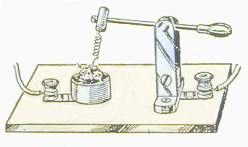
The idea of the passive receiver is more than 100 years old. The first receiver type that is known to detect radio energy is the coherer type. The coherer invented by Edouard Branly and it is a primitive form of radio signal detector, used in the late 19th century, consisting of a capsule of metal filings in the space, sometimes evacuated, between two electrodes. It was a key enabling technology that led to radio, and was the first device used to detect radio signals in practical spark gap transmitter wireless telegraphy. Below is a typical schematic of a coherer type receiver.
Although
the coherer is satisfactory for responding to the "on-off keying"
characteristic of an early spark gap transmitter, it cannot follow the
complex waveforms of audio broadcasting.
This problem was solved by the
demodulation
capability enabled by the hot wire barretter and the electrolytic
detector.
Although the coherer is satisfactory for responding to the "on-off
keying" characteristic of an early spark gap transmitter, it cannot
follow the complex waveforms of audio broadcasting. This problem was
solved by the demodulation capability enabled by the hot wire barretter
and the electrolytic detector. Years later he invented the demodulating detector in
1902 that found limited use in early radio receivers. In effect it was
a highly sensitive thermo resistor developed to permit the reception of
amplitude modulated signals, something that the coherer (the
standard detector of the time) could not do.
The hot wire barretter was a demodulating detector invented in 1902 by
Reginald Fessenden that found limited use in early radio receivers. In
effect it was a highly sensitive thermo resistor developed to permit
the reception of amplitude modulated signals, something that the
coherer (the standard detector of the time) could not do.
The first device used to demodulate audio signals, it was later
superseded by the electrolytic
detector,
also generally attributed to Fessenden. The electrolytic detector,
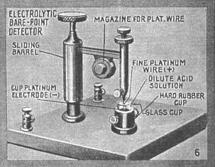
or
the bare-point electrolytic detector as it was also called, was a type
of wet demodulator used in early radio receivers. This form of detector
was in extensive use, and was very sensitive and reliable.
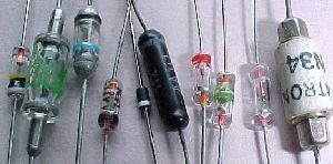
The last and most known part of passive ratio came with the crystal detector. Cat’s whisker crystal detector refers to a thin wire that lightly touches a semi conducting crystal to make an imperfect contact-junction detector in a crystal radio. While originally a figurative description of a mechanical part, the term grew to encompass the entire detector assembly and also in some English speaking communities to describe the receiver itself.
Since then, the technology has been advanced and the materials that composed the crystal detector were packaged into small parts called diodes. One of the most common materials used for the diodes is germanium and so these diodes are called germanium diodes or germanium detectors.
Introduction
Passive
receivers have been always fascinated people. The absence of electrical
power and the simplicity of the circuits were two of the most important
reasons. Other reasons may include the nostalgia for the old, the
beauty of the sets and the cabinets etc. In this page I present you the
research that I did using internet resources in my try to build a
superior crystal receiver. I have been based only on internet resources
and it took me one week of continuous search to understand the
different circuit topologies and the basics behind the crystal
receiver. I made a search package zipped of around 150Mb size. It is
available for you upon request. Instead of presenting you the super
duper circuit and try to convince you that it is the best (as some home
brewers will do), I will try to explain you the reasons why my
schematic approach is superior to many others.
I am a person of the new generation but I personally like the way some
things were built at the past, but I also consider the disadvantages
and the bad points (where they existed) of some of the circuits of this
era. I am not the person that will give an ironic look to the many
decades home brewers' constructions and I highly respect their opinions
but... some things have to be better than the classical way of making
them. I always try to support my opinion with arguments and I do not
blindly believe a construction to be good if I do not try it myself.
That is how I am going to approach the topic in this article.
I am not going to give lot of theory behind this consideration because
I want to keep the page simple for the reader. Everything, including
the theory, is on the search package for you to read if you want so. Of
course nothing is perfect and there is a lot of experimentation that
can be done in order to achieve even better results. I will greatly
appreciate your comments on any part of the text, at my email address
at the beginning of the page.
First
of all a few introductory words about crystal receivers.
Crystal receivers are passive devices. The term passive means that they
do not use any other electrical power apart from the one that comes
from the antenna, i.e. the radio signal. If a receiver fails to follow
this rule it cannot be considered as passive.
Crystal receivers cannot achieve any type of amplification (except from
some special cases that will be presented in this page). The energy of
the out coming signal will always be lower than the energy of the
incoming, mainly because of the losses of the different parts of the
receiver. One main goal of the experimenter is to minimize these losses
as much as possible in order to achieve more signal at the receiver
output.
Do not expect great performance by any crystal receiver. The best
crystal receiver you can find will be much more inferior to a simple
pocket radio of today's technology. I am not telling this to disappoint
you but it is the truth. The superheterodyne topology itself is much
more inferior than the envelope detector used in crystal receivers.
Unless you really need a set that will operate without power and you
are able to have a big antenna and good earth, do not go for a crystal
receiver, as far as concern performance issues.
After all this introduction let's come to the point of the page.
Sensitivity versus selectivity
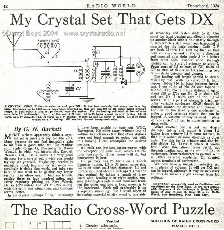
Crystal-set DXers are up against two problems: selectivity versus sensitivity. Sensitivity describes the ability of the receiver to receive weak signals. The more sensitive a receiver is, the weaker signals it can receive. Selectivity is the ability of the receiver to distinguish a wanted signal from unwanted others, so you can listen to only this signal and not the unwanted ones. If you have not any means of filtering in your receiver, maybe you could make it more selective by lowering it's sensitivity. But then you would not be able to hear the weaker stations but only the loud ones. Also if two loud stations are close together in frequency, lowering the sensitivity, would not necessarily improve the selectivity. If you live in a city or near a large city that has several AM signals, your main focus will be on separating signals so that the weaker DX can be heard between the blowtorches. On the other hand, if you live in the country, you don't have to worry so much about separating strong locals; you can run things 'wide-open' enabling you to log some of the weaker DX signals. Living away from the city certainly makes life simpler for crystal radio DXing but don't despair if you are a city-dweller.
Topologies of crystal receivers
There are many topologies that can be used in crystal receivers but all of them consist of some main parts. There is always an antenna and an earth, a means of selectivity, a means of detection and a means of audio conversion. The selectivity part is usually composed of coils and capacitors and its purpose is to select the desired signal among unwanted ones. The detection part is usually composed of a detector (crystal ore or diode) and its purpose is to convert the high radio frequency signal to low audio frequency one. The audio conversion part is usually composed of headphones or other devices and its purpose is to convert the audio waveform into air pulses (i.e. sound) for your ears to listen. Below I will present you some basic topologies of crystal receivers that I have come across.
The
diagram shows a simple basic crystal radio. It is probably the simplest
you can find.
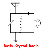 In the city, with a good
antenna, such a set will hear plenty of locals but it is unlikely to
hear any DX. Take it out to the campground for the weekend however and
even a simple set like this is capable of logging DX. Since most of us
live in or near the city, we need to look at ways of transforming the
basic set into a DX machine!
In the city, with a good
antenna, such a set will hear plenty of locals but it is unlikely to
hear any DX. Take it out to the campground for the weekend however and
even a simple set like this is capable of logging DX. Since most of us
live in or near the city, we need to look at ways of transforming the
basic set into a DX machine!
In order to
separate the strong locals, the tuned circuit (L-C) must have as high a
'Q' as possible. Q, the quality factor of a coil, is the ratio of the
inductive reactance (i.e. "AC resistance") of a coil at a particular
frequency to the resistive losses of the coil. This resistive component
is the sum of the DC resistance and other losses such a dielectric
losses in non-conductive material close to the coil and eddy-current
losses in nearby conductors or the coil wire itself. High Q not only
yields better selectivity, but also raises the impedance of the tuned
circuit, which can allow more voltage to be applied to the detector.
Placing the diode and headphone load at the top of this circuit will
result in strong signals but poor selectivity. The impedance of the
headphones will load down the tuned circuit, lowering its 'Q'. The
result is very poor selectivity.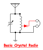 Tapping the diode/headphone load at a lower point in the tuned circuit
results in less 'Q-lowering' of the circuit. The result is a higher
degree of selectivity. You don't, however, get a free ride! The higher
selectivity diode tap point results in less overall voltage being fed
to the headphones. Signals are weaker but easier to separate! The
challenge of building an efficient tuner is to find the right balance
between selectivity and sensitivity!
Tapping the diode/headphone load at a lower point in the tuned circuit
results in less 'Q-lowering' of the circuit. The result is a higher
degree of selectivity. You don't, however, get a free ride! The higher
selectivity diode tap point results in less overall voltage being fed
to the headphones. Signals are weaker but easier to separate! The
challenge of building an efficient tuner is to find the right balance
between selectivity and sensitivity!
There
are a few more improvements that will help the 'basic set'. More
sensitivity as well as more selectivity can be realized in the antenna
circuit. A separate antenna coupling coil that will couple the antenna
into the main tuning coil will result in a further overall improvement.
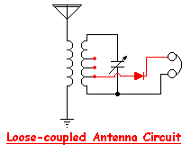 If the position of the
antenna coil can be adjusted in relation to the main tuning (detector)
coil, a degree of coupling can be reached that offers a good balance
point between adequate sensitivity and improved selectivity. Often the
antenna coil and the detector coils are mounted on a long rod or dowel
that allows easy adjustment of the 'loose-coupling' circuits. Also note
that improved detector tuning can be achieved by optimizing the diode
'tap' location on the main tuning coil.
If the position of the
antenna coil can be adjusted in relation to the main tuning (detector)
coil, a degree of coupling can be reached that offers a good balance
point between adequate sensitivity and improved selectivity. Often the
antenna coil and the detector coils are mounted on a long rod or dowel
that allows easy adjustment of the 'loose-coupling' circuits. Also note
that improved detector tuning can be achieved by optimizing the diode
'tap' location on the main tuning coil.
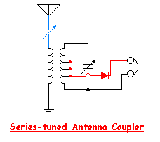 Further improvements in both
sensitivity and selectivity can be achieved by actually tuning the
antenna system to resonance. Your type of antenna system as well as the
part of the AM band that you are tuning will determine which system
works best. The series-tuned antenna coupler is best suited for tuning
large antennas, especially those with large horizontal runs ("top
hats"). The parallel-tuned antenna coupler is better suited for tuning
shorter antennas, such as vertical wires, masts or whips - those
without top hats.
Further improvements in both
sensitivity and selectivity can be achieved by actually tuning the
antenna system to resonance. Your type of antenna system as well as the
part of the AM band that you are tuning will determine which system
works best. The series-tuned antenna coupler is best suited for tuning
large antennas, especially those with large horizontal runs ("top
hats"). The parallel-tuned antenna coupler is better suited for tuning
shorter antennas, such as vertical wires, masts or whips - those
without top hats.
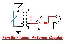 A series of test clips or a
simple switching system can be used experimentally to determine what
works best for you. Making this effort is important
as it goes a long way towards avoiding initial disappointment with the
crystal set's performance. Such a system as this is called a
'double-tuned' set. With care and attention to construction, such
systems are capable of hearing DX signals.
A series of test clips or a
simple switching system can be used experimentally to determine what
works best for you. Making this effort is important
as it goes a long way towards avoiding initial disappointment with the
crystal set's performance. Such a system as this is called a
'double-tuned' set. With care and attention to construction, such
systems are capable of hearing DX signals.
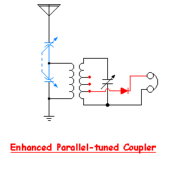 Adding a tuning capacitor in
series with the antenna permits a long antenna to be tuned very
effectively by a parallel-tuned antenna coupler. In fact, this is the
method-of-choice for many crystal set listeners. To avoid the
complication of an extra tuning knob, a single-knob, two-gang variable
capacitor can be used as shown here. The added variable capacitor can
be placed instead in the ground leg. This 'enhanced parallel-tuned'
coupler can be very effective in peaking up desired signals while
knocking down nearby interference. The use of a tapped coil in this
circuit can be very beneficial in achieving optimal Q for the portion
of band being tuned. One might even decide on using separate
'high-band' and 'low-band' coils for this circuit.
Adding a tuning capacitor in
series with the antenna permits a long antenna to be tuned very
effectively by a parallel-tuned antenna coupler. In fact, this is the
method-of-choice for many crystal set listeners. To avoid the
complication of an extra tuning knob, a single-knob, two-gang variable
capacitor can be used as shown here. The added variable capacitor can
be placed instead in the ground leg. This 'enhanced parallel-tuned'
coupler can be very effective in peaking up desired signals while
knocking down nearby interference. The use of a tapped coil in this
circuit can be very beneficial in achieving optimal Q for the portion
of band being tuned. One might even decide on using separate
'high-band' and 'low-band' coils for this circuit.
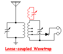 Although you may now be able to hear some DX,
chances are you are still bothered by at least one (if not several)
local 'pest' signals. Further gains in selectivity can be had by the
addition of another tuned circuit, called a 'wavetrap'. By coupling
this circuit to the detector coil, this circuit can be tuned to the
same frequency of the pest signal, absorbing much of its signal-killing
strength at the detector, while not adversely affecting the strength of
wanted signals. More than one wavetrap may be employed to tackle more
than one pest signal. With a high Q wavetrap, very loose coupling is
usually best.
Although you may now be able to hear some DX,
chances are you are still bothered by at least one (if not several)
local 'pest' signals. Further gains in selectivity can be had by the
addition of another tuned circuit, called a 'wavetrap'. By coupling
this circuit to the detector coil, this circuit can be tuned to the
same frequency of the pest signal, absorbing much of its signal-killing
strength at the detector, while not adversely affecting the strength of
wanted signals. More than one wavetrap may be employed to tackle more
than one pest signal. With a high Q wavetrap, very loose coupling is
usually best.
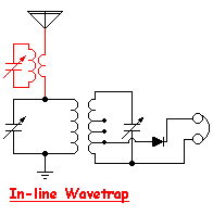
Another method that some find successful is the use of an 'in-line'
wavetrap in the antenna circuit. The smaller secondary winding can be
wound either on top of the primary or on one end. One or two in-line
wavetraps can often be used to effectively knockdown the strong pest
signals.
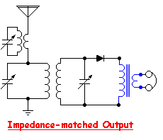 Another important improvement
can be made in the headphone circuit. If you are using the old standard
style of headphones (Brush, Baldwin etc) they must be high impedance
phones. The modern low-impedance 'walkman' style phones will load-down
the detector circuit too much, seriously degrading selectivity and
signal strength. Even high impedance phones will cause unwanted loading
of the detector circuit. Using a low-loss audio transformer with a very
high impedance primary between the phones and the detector will reduce
the problem and often great gains in selectivity can be achieved.
Another important improvement
can be made in the headphone circuit. If you are using the old standard
style of headphones (Brush, Baldwin etc) they must be high impedance
phones. The modern low-impedance 'walkman' style phones will load-down
the detector circuit too much, seriously degrading selectivity and
signal strength. Even high impedance phones will cause unwanted loading
of the detector circuit. Using a low-loss audio transformer with a very
high impedance primary between the phones and the detector will reduce
the problem and often great gains in selectivity can be achieved.
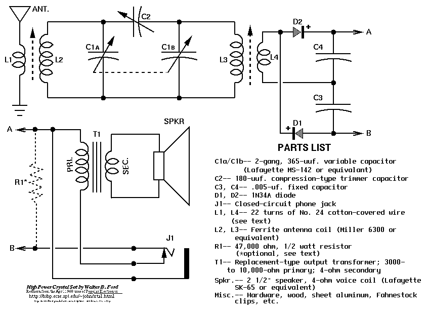
This
is the schematic diagram of a good performance receiver based on the
above considerations.
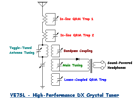
This is a 'triple-tuned' arrangement. There are vernier reduction
drives on all tuning capacitors as tuning is very sharp on all
circuits. Because of the great abundance of 'blowtorch' signals within
15 miles of my location (seven 50 KW locals) heavy trapping of pests is
required. Both sensitivity and selectivity are quite good.
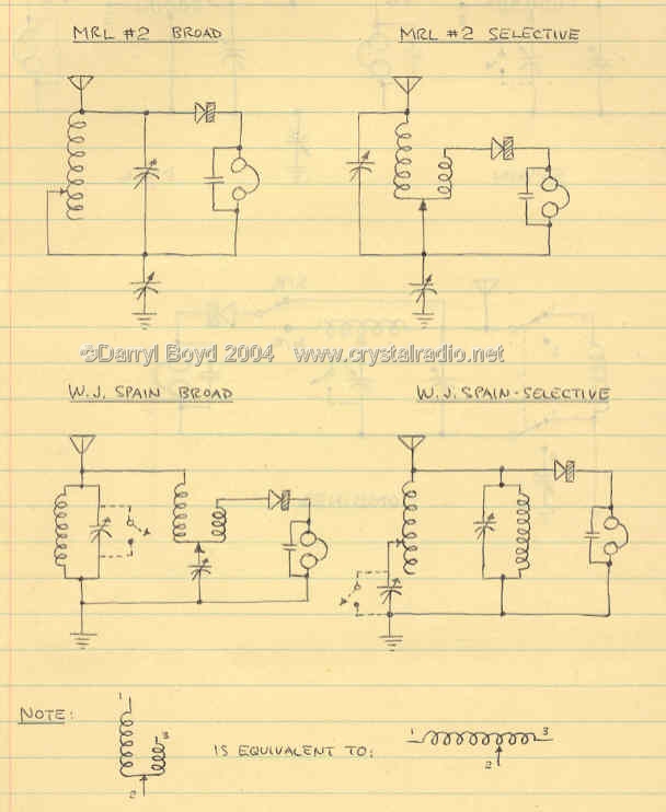
Below many other additional approaches are presented. There is no
better description than the original articles so please click on each
picture to view or download the relevant article.
The second picture below uses a band pass filter to select the desired
station. The fourth picture uses a wave trap and offers both broad and
selective tuning to be made.

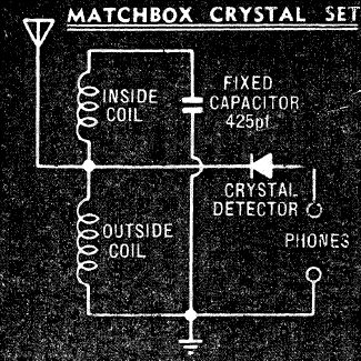
More classic schematics.
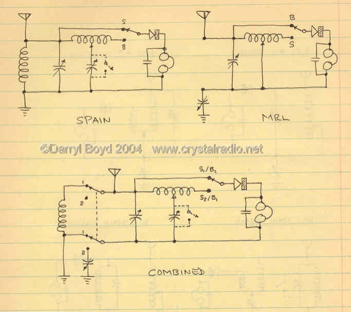
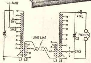
The schematic below uses double tuned circuits linked together by a link line, so it could be build in two boxes maby.
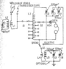
The three schematics below incorporate the use of a variometer (variable coil inductively varied, not selective).
Many other circuits in the boy's book of crystal sets.
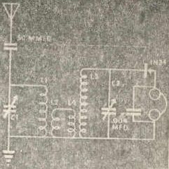
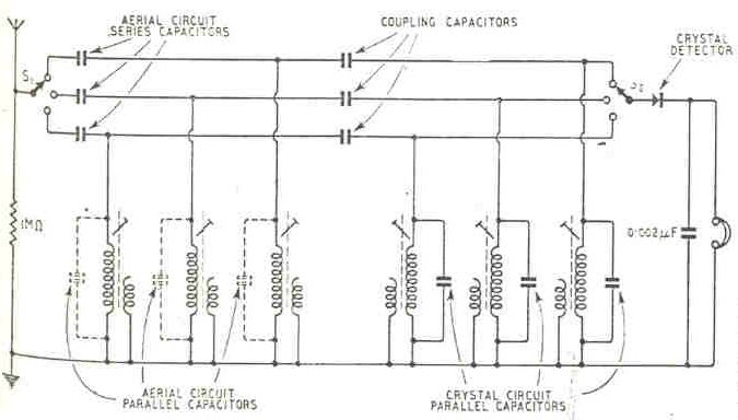
The next seven circuits use band pass filters in order to improve selectivity. A band-pass filter is a device that passes frequencies within a certain range and rejects (attenuates) frequencies outside that range. These filters can be created by combining a low-pass filter with a high-pass filter and that is the case here. Band pass filters are quite sharp and they are used extensively not only in crystal radio but in all forms of receivers.


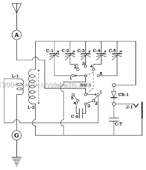
The next three circuits show you how you can construct your crystal receiver in order to have memories of pre-selected stations. A crystal receiver can have memories? Of course it can. Not electronic memories but rather a set of multiple tuned circuits, each one tuned to a predetermined station in the band. Using a multi-switch you can select the desired stored station by selecting the relevant tuned circuit. That is a clever technique but it requires you to multiply the tuned circuits of the receiver by the number of the memories you want to have.
Up
to this point I have shown you most of the more conventional crystal
receiver topologies. Now I am going to show you a different approach to
the topic. The next circuits could be described as more modern circuits.
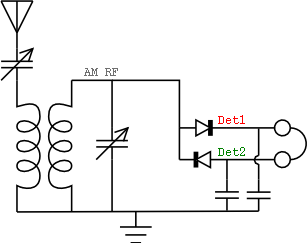
In a conventional crystal receiver the diode delivers power to the
headphone during the positive part of the RF cycle. The negative part
of the RF cycle goes nowhere. We went to all the trouble to put up a
100 foot antenna and then waste half the energy we manage to capture.
In the first picture below the top diode delivers power to the
headphone during the positive part of the RF cycle and the bottom diode
delivers power during the negative part of the RF cycle. In your
typical crystal radio the voltage across the headphone comes from Det1
and ground (0 volts), so it has a magnitude equal to that of Det1. By
putting the voltage from Det2 at the other side of the headphone, we
get a difference of Det1-Det2 across the headphone (i.e. a greater
voltage). Of course, this isn't exactly how it works. Really, the
forward voltage drop of the diodes has a big effect on the output
voltage, and all kinds of impedance interactions probably show up when
you hook up another detector. So I do not know how efficient this
circuit can be. But, this should get the idea across. A person could go
through a lot of math to figure out exactly what happens. I think it's
easier and more satisfying to just build the thing and see how good it
works.
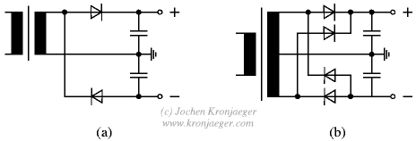
The next two circuits use another technique called voltage doubling to double the voltage that comes into the headphones. These are generally more effective detectors.
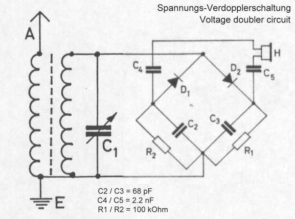
In order to understand better the how voltage doubling works consider the following. There are two types of voltage doublers. The Greinacher and the Villard.
|
|
Greinacher voltage doubler circuit. (a) simple version for grounded input voltage, (b) double version for symmetric input voltage. Diodes must be dimensioned for 2x input peak voltage Up, caps only for 1x Up. |
The Greinacher doubler circuit (a) transforms a grounded AC voltage (peak voltage Up) into symmetrical DC voltages of 1x Up each, thus producing 2x Up between outputs. If the input voltage is already symmetrical (e.g. as in an Obit), the Greinacher circuit may be doubled according to (b). This does not change the output voltages but increases the possible output current by a factor of two.
|
|
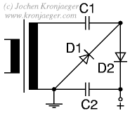
Villard voltage doubler circuit for positive polarity towards ground. For negative polarity reverse all diodes. Diodes and caps must be dimensioned for 2x Up. For sinusoidal input voltage 1x Up is sufficient for C1. |
In contrast to the Greinacher circuit, the Villard doubler circuit produces 2x Up towards ground at a single output. Besides this, the advantage of the Villard circuit is that it may be cascaded to form a voltage multiplier with (in principle) arbitrary output voltage. The way this works is that after C1 and C2 are fully charged to 1x and 2x Up respectively, there is a pulsating DC voltage oscillating between 0 and 2x Up across D2, which is converted to AC by the subsequent cap and thus acts as input AC of the next stage, and so forth.
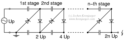
|
|
Cascaded Villard doubler circuits. All diodes and caps must be dimensioned for 2x Up. For sinusoidal input voltage, C1 of the first stage may be reduced to 1x Up. |
The next three circuits are examples of another type of detection, the full wave detection. These are not similar to the double diode circuits described above and they do not use the previously mentioned voltage doublers, yet they are very efficient and they provide some advantages over the voltage doubler circuits that will be discussed later on.
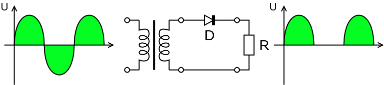
In half wave rectification, either the positive or negative half of the AC wave is passed, while the other half is blocked. Because only one half of the input waveform reaches the output, it is very inefficient if used for power transfer. Half-wave rectification can be achieved with a single diode in a one phase supply, or with three diodes in a three-phase supply.
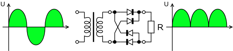
A full-wave rectifier converts the whole of the input waveform to one of constant polarity (positive or negative) at its output. Full-wave rectification converts both polarities of the input waveform to DC (direct current), and is more efficient. However, in a circuit with a non-center tapped transformer, four diodes are required instead of the one needed for half-wave rectification. This has some disadvantages that we will see later on. Four rectifiers arranged this way are called a diode bridge or bridge rectifier:
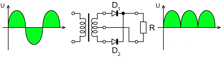
For single-phase AC, if the transformer is center-tapped, then two diodes back-to-back (i.e. anodes-to-anode or cathode-to-cathode) form a full-wave rectifier (in this case, the voltage is half of that for the non-tapped bridge circuit above, and the diagram voltages are not to scale). However this is a very good case for the crystal receiver for reasons that will be discussed later on.
I said earlier that crystal receivers cannot achieve any type of amplification, except from some special cases. The next notes and schematics have to be considered with great interest. They achieve amplification without using external power other than the one comes from the antenna. They are still crystal receivers and they still use detectors. The diodes here, are not used for signal detection but they deliver power to the transistor amplifier/detector. One could argument that this may degrade the wanted signal. But what is actually happening is that the power needed for the transistor is not taken from the wanted signal itself but from the unwanted ones that the antenna receives. In this case, the greater the RF interference in an area, the better.
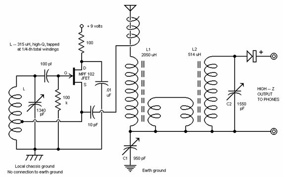
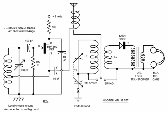
Two other examples of such receivers are shown below. They use FETs as RF amplifiers and detectors. I do not know if they use unwanted or wanted signals for the power required for the FETs to work and I am not sure if they can be considered as crystal receivers as they do not use any diodes or germanium transistors. But nevertheless, the topic of the project is not only about crystal receivers but generally about passive receivers. The rectification is done by the FET itself. Well no one says that a crystal receiver must use only diodes or germanium transistors for detection, although the word "crystal" denotes this. In the context that they do not use external power they can be considered as crystal receivers but in the context that they do not use diodes/germanium transistors for rectification they cannot. The certain thing is that they do not use external power and this makes them passive. They also offer some advantages over diode crystal sets.
Here you can find more details of how to build such circuits
Below there are some more schematics and descriptions (above them) about such circuits.
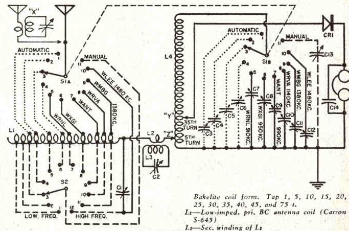
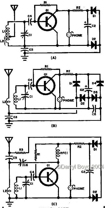
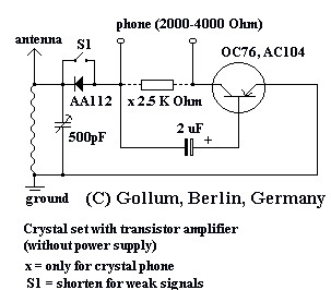
Simple Crystal set for local transmitter
You can use also a crystal phone (x = 3 K OHM). For weak signals you can shorten the amplifier switch. Transistors: AC151, AC104, OC76, SB187. Rectifiers: AA112, AA114, AA132, OA85. L= 100 or 120 wdg with diameter 2 cm, C= 500pf for MW.
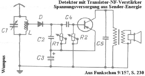
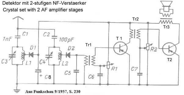
Crystal receiver with AF-amplifier for your local broadcast transmitter. Model 1
The rectified RF is smoothed with R1 and C3 and is the "source" for the voltage energy of the AF - transistor. Disadvantage of the receiver: The voltage stands only at strong transmitter at the disposal. On the other hand is loudspeaker - reception realizable. L= 100 or 120 wdg with diameter 2 cm, C1= 500pf, C2= 1nf, C3= 3uf, C4= 0.1 uf, C5= 500 500pf, R1= 1M, R2= 1M, transformer 6/1 or 4/1, transistor: AC151, AC104, OC76, SB187 rectifier: AA112, AA114, AA132, OA85.
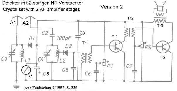
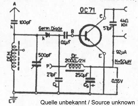
Crystal receiver with AF-amplifier for your local broadcast transmitter. Model 2
The second concept is more profitable. The transistor - energy is produced from a separate resonance-circuit. This circuit (L1/C3) is tuned firmly on the local transmitter, Circuit C4/L2 is tuned for radio reception. Good loudspeaker - reception, also at weaker transmitters, is the result. As transistors are indeed germanium - types necessary. You need a operation voltage of about 800 mV at C8 for well working.
Transistors: AF preamplifier T1 = OC71 ( NKT214, 2N280, 2SB244) , AF final amplifier T2 = OC 72 (2SB56, NKT212, 2N281). R1 = 75 KOhm, R2 = 100 KOhms, C8 = 100 uF, C5 = 500 pF, C6 und C7 = 10 uF, transformer Tr1 = 1/1 ratio Z approx. 4000/4000 Ohms, transformer Tr2 = 2/1 ratio Z =2000/1000 Ohms, transformer Tr3 = Z 200/4-5 Ohms. L1 and L 2= 100 wdg with diameter 2 cm (tap for D1 80 wdg from ground) , C3/C4= 500pf, rectifiers: AA112, AA114, AA132, OA85. I think, you have problems to buy the transformers. Perhaps you find an old low price transistor portable with some transformers.
Adjust the trimmers R1 and R2 for best audio quality (bias voltage between basis and emitter of approx. 350-450 mV).
Version 2: For best performance use separate antennas for power supply detector and receiver detector. L1 except tap. A1 for power supply detector. C9 = ceramic 1nF. With the (high ohm) voltage meter you can adjust to highest voltage. Use a instrument with a full range of 3 to 10 V in relation to the max. voltage on your location..
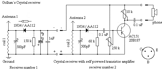
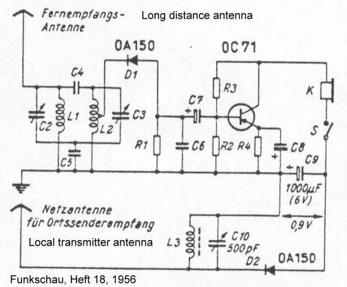
Crystal receiver with AF-amplifier also for long-distance broadcast reception.
This is a high performance project because the supply voltage needed for the transistor amplifier is generated by the local broadcast station to which crystal receiver number 1 (left side of the schematic) is fix-tuned. Tune with the aid of a meter and adjust for maximum detection. Good AF amplification also of low-level stations with the crystal receiver number two (right side of schematic). Use a Germanium low signal AF type transistor (AC151 or 2SB187, etc.). A supply voltage as low as 450 mV produces audible signal amplification. Of course you have to use TWO antennas.
I use for the crystal receiver number 2 (right) a loop (frame) antenna, for crystal receiver number 1 (left) I use a 20 meters (66 feet) wire outside antenna. This generates a supply voltage of approx. 900 mV under load of receiver number 2.
Adjust the variable 250 k ohms resistor to approx 50 % of the voltage generated by receiver number 1 voltage (measured at + pole). Best value for 10 k ohms trim pot is 3 to 6 k ohms.
Do not use electrolytic for the 0.1 uF capacitors. Do not forget to install the 1 nF capacitor. The 150 k ohms resistor of receiver number 1 is not really necessary. Attention for the polarity of the diode in receiver number 1.
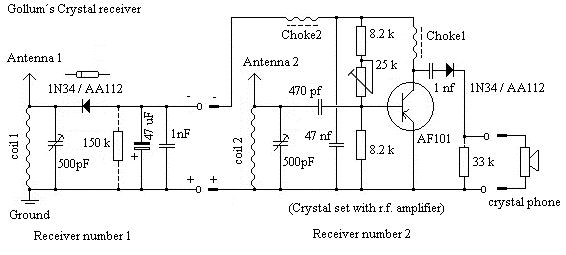
Crystal receiver with RF-amplifier for long-distance broadcast reception.
This concept is effective since the supply voltage for the transistor amplifier is provided by a separate tuned circuit which is fix-tuned to the local radio station and thus is constantly available (tune to maximum output with a suitable meter). Unlike the previous circuit this time the radio frequency is amplified, not the audio frequency. This concept is more suitable for long distance reception.
Good sensitivity by rf amplification. The transistor required is a germanium rf type (an AF101 or 2SA175 or other rf type). Already a voltage of about 450 mV produces audible amplification. You will HAVE TO USE two separate antennas. Coils used have ferrite (powered iron) cores, variable capacitors are solid dielectric types with 500 pF. The rf chokes (RFC 1 and 2) may be made by winding about 200 turns of this enameled copper wire on a ferrite slig with a diameter of 10 and a length of 50 millimeters.
For detector receiver number two I used at night-time a loop antenna and for detector radio number one (left side of schematic) I use an out-side wire antenna of 20 meters length. This set-up produces a voltage of about 900 mV under load of the second detector set.
Adjust the 25 k-ohms trimmer for the loudest signal.
The 150 k-ohms resistor is not really necessary. Watch the polarity of the diode in the receiver number 1.
For 2000 ohms magnetic headphones
For 4-5 ohms earphone
For 2000 ohms magnetic headphones
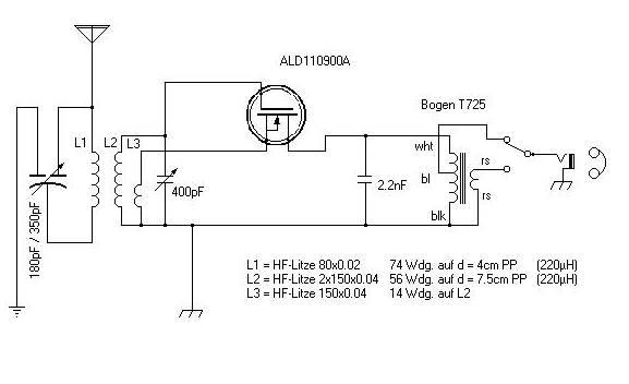
SW-band crystal set with transistor AF amplifier powered by the transmitter energy.
An
alternative use of a battery is possible. A second receiver for MW band
delivers the voltage for the transistor amplifier. With S2 you can
connect the headphones direct to the crystal set or to the output of
the AF transistor amplifier. The 20 uA measuring instrument is for best
tuning of the SW broadcast station. 2000 ohms headphones.
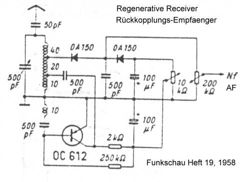
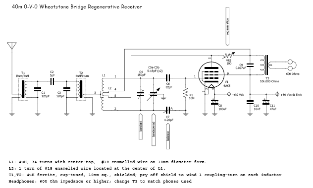
Another type of such radio that describes a vacuum tube Wheatstone Bridge 0-V-0 Regenerative Receiver with Passive hybrid reverse antenna isolation
All the crystal receivers described above are able to detect only AM (amplitude modulated) signals. The next circuits are definitely not crystal receivers. They use a combination of a passive and an active circuit. The reason why I present them to you is that they are capable of demodulating SSB (single side band) signals. If one could make the BFO taking power from the antenna, like the circuits I presented above, then these would be SSB crystal sets. This is a very good point of experimentation for someone that would like to try.
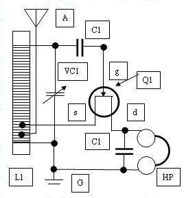
The Omega receiver
In
searching for the superior passive receiver I decided to create the
Omega project. The Greek letter Omega (
![]() ) was used for some reasons, including my
admiration for Ancient Greeks. I would lie to you if I said that I have
already constructed the most efficient passive receiver already. This
is a topic of much discussion and experimentation throughout the years
and maybe decades. This is exactly what I am going to do in this page.
But like every project it has to start somewhere. Your support and
thoughts are greatly appreciated. Send me an email if you have anything
to say about the topic, and who knows, we may discover other
fascinating things related not only to this, but generally to
electronics!
) was used for some reasons, including my
admiration for Ancient Greeks. I would lie to you if I said that I have
already constructed the most efficient passive receiver already. This
is a topic of much discussion and experimentation throughout the years
and maybe decades. This is exactly what I am going to do in this page.
But like every project it has to start somewhere. Your support and
thoughts are greatly appreciated. Send me an email if you have anything
to say about the topic, and who knows, we may discover other
fascinating things related not only to this, but generally to
electronics!
A receiver of this type must have the advantages of the topologies
described above and minimize the disadvantages. It must be definitely a
combination of some of the above circuits and it has to extend somehow
to new ideas and approaches. But first let's just start from the
basics.
Instead
of starting from the RF selectivity or the antenna stage, I am going to
start from the other way round, the detector. Every receiver must have
some kind of detector. A good receiver must have an efficient detector.
There are a few types of detectors but here I will present a few things
about diode detectors. We have already seen these types of detectors
but here I will give a betted approach based on their advantages and
disadvantages. If a large off-balance output voltage (2-20V RMS) is
available, the detector can be one of a variety of simple diode
rectifier circuits. Although, as we will discuss shortly, consideration
must be given to the type of diode used. Note that for any of the diode
detector circuits shown below, the polarity of the DC output can be
reversed by reversing all of the diodes.
Half-wave
rectifier
The simplest detector of all is the half-wave rectifier circuit shown
below:
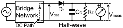
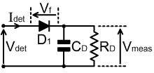
| The
DC output of this detector, i.e., the measured voltage Vmeas, is approximately Vdet��2 , where Vdet
is the magnitude of the AC voltage appearing at the detector port;
i.e., Vdet=|Vdet| . The output is equal to the
peak value of the input voltage provided that the detector load
resistance RD is high in
comparison to the output impedance of the bridge network, and provided
that Vdet is large in
comparison to the forward voltage drop of the diode D1.
In this notional diagram, RD
is shown as being separate from the meter, and the meter is assumed to
be a perfect voltmeter, i.e., of infinite resistance. In practice, RD is usually the resistance of a real
voltmeter constructed by placing a resistor in series with a
microammeter. For example, a 100mA meter padded-up to 10KW by means of
a series resistor makes a 1V FSD (full-scale deflection) voltmeter. The
smoothing capacitor CD should
be chosen so that the time-constant CD�RD is at least 10 times the period
(1/f) of the lowest frequency at which measurements will be made. If
the lowest frequency is to be, say, 1MHz and RD=10KW,
then we want CD�RD to be greater than 10ms, i.e., CD>1nF. If a meter is used as
the indicator, it makes no practical difference if the capacitor is
somewhat larger than the minimum required, and so 0.1mF (ceramic disk)
is a typical choice; but very large capacitors (10mF and more) will
damp the meter response and may make it difficult to locate sharp
nulls. Note incidentally, that if the signal generator is amplitude
modulated (e.g., with a 1KHz sine wave), and the time-constant CD�RD
is chosen to be shorter than the period of the modulating frequency
(e.g., about 100ms or 10KW in parallel with 10nF), then the indicator
may be a high-impedance (e.g. piezo-crystal) earphone, or an audio
amplifier and loudspeaker. The reverse voltage rating for the detector diode (VRM) can be determined by noting that CD is charged to a constant voltage approaching Vdet�2, whereas the most negative instantantaneous voltage appearing at the detector input is -Vdet�2. Hence the diode must have a VRM of at least 2�2 (i.e., 2.818) times the maximum possible RMS input voltage.
One drawback of the half-wave rectifier circuit is that it will give no output unless there is a DC path through the network from which it receives its drive. In many bridge circuits, there will be no such path, and the traditional solution to this problem is to place an RF choke across the input to the detector. The choke should have a reactance which is high in comparison to the detector load resistance at the lowest frequency of operation. 3.5mH is a typical choice, and has a nominal reactance of about +40KW at 1.8MHz. However, a practical inductor also has substantial self-capacitance; and this will resonate with the inductance at some frequency, and overwhelm the inductance at frequencies higher than the self-resonance frequency. The result will be a peak in detector sensitivity followed by a falling frequency response. Capacitance effects in the frequency-range of interest are not necessarily a problem if the choke is well designed, but they cannot be guaranteed to be inconsequential without practical verification. In general, insofar as the use of chokes cannot be avoided, an RF choke composed of multiple segments (pie-wound) gives the highest self-resonance frequency (SRF) and so is to be preferred. |
Shunt-diode
rectifier
A half-wave rectifier can also be constructed using the shunt diode
configuration shown below.
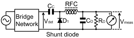
| This
circuit appears, at first glance, to place a diode across the detector
port; but it does no such thing because of the action of the coupling
capacitor CC. When the bridge
output Vdet
first goes negative (relative to the polarity arrow shown on the
diagram), D1 conducts and
clamps one end of CC to
ground, causing the capacitor to be charged to the negative peak value
of Vdet (i.e., -Vdet��2). The charge in CC then remains reasonably constant on
the time-scale of the AC signal, and so the near-sinusoidal voltage at
the cathode of D1 averages
about +Vdet��2 instead of
zero. The filter comprising the RF choke and CD
removes the AC component to give a measured voltage of Vdet��2 (neglecting the loading due to
RD), which is the same as for
the ordinary half-wave detector. Since D1
only conducts to keep CD
topped-up rather than throughout the entire negative half-cycle of Vdet, the input impedance of the shunt
diode detector is similar to that of the normal half-wave detector.
With regard to the use of an RF choke however, the same caveats as
before apply; but note that if the meter has greater sensitivity than
needed to give a good indication of Vdet,
then the overall sensitivity of the detector can be reduced by
replacing the RF choke with a resistor, and the troublesome choke is
then eliminated. Since the voltage at the cathode of the diode averages at +Vdet�2, the instantaneous peak inverse voltage sustained by the diode will be Vdet2�2. Hence, as in the case of the simple half-wave rectifier, the VRM for the diode must be at least 2�2 times the maximum possible RMS input voltage.
Due to the need for the coupling capacitor CC, the component count of the shunt diode circuit is potentially higher than that of the half-wave detector. If the bridge has a capacitive voltage-divider network however, the role of the coupling capacitor is performed by the voltage splitter and CC is not required; in which case the component count is the same as before. If there is any DC path across the detector port however, CC is essential; and if needed it should be chosen to have a reactance which is always small in comparison to the detector load RD. If the lowest frequency of operation is say 1MHz and RD is 10KW, then the voltage drop across the capacitor will be negligible of its reactance is always less than 1% of RD, i.e., less than 100W at 1MHz. Since C=1/2pfXc, we may calculate that CC should be at least 1.6nF. Once again, it makes no practical difference if the capacitor is somewhat larger than the minimum required, and so 10nF (0.01mF) is a sensible choice. |
Voltage-doubler rectifier
Given that RF chokes are bulky and potentially problematic, it is often
sensible to try to avoid using them even if sensitivity is paramount
(i.e., in situations where the choke cannot simply be replaced by a
resistor). This can be done in various ways; the first example, shown
below, being known as a 'voltage doubler'. This is a Villard voltage
doubler. A Greinacher voltage
doubles has been discussed in a previous section of the page.
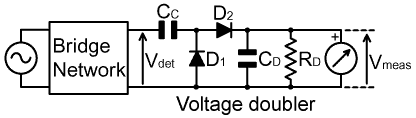
| In
this case, the RF choke of the shunt-diode detector is replaced by a
another diode D2. As before,
the coupling capacitor CC can
be omitted if there is a DC open-circuit looking back into the RF
source. The output of the voltage doubler, Vmeas,
is approximately Vdet�2�2,
the reason being as follows: When Vdet first goes negative, D1 conducts and clamps one end of CC to ground, causing the capacitor to
be charged to -Vdet��2. The
charge in CC then remains
substantially constant on the time-scale of the AC signal, and so the
voltage across CC is placed
in series with Vdet,
ultimately causing the smoothing capacitor CD
to be charged, via D2, to
approximately twice the peak value of Vdet (provided that RD
is very large in comparison to the output impedance of the bridge
network). Since this detector conducts on both positive and negative
half-cycles of Vdet,
it is actually a type of full-wave rectifier. Due to the clamping action of D1, the voltage at the anode of D2 cannot fall substantially below zero. Hence, since the voltage across CD is +Vdet2�2, VRM for D2 must be at least 2�2 times the maximum possible RMS value of Vdet. In the case of D1, since Cc is charged to -Vdet�2 and the maximum instantaneous negative excursion of the input voltage is also -Vdet�2, then VRM for D1 must also be at least 2�2 times the maximum possible RMS value of Vdet.
One problem with the voltage doubler, is that there are effectively two diodes in the path to the meter, and consequently the output is reduced by two diode forward voltage-drops. This is not so good for crystal receivers and it also makes the detector less linear than the previously discussed half-wave rectifiers. Non-linearity is not necessarily a serious issue when making null measurements; but later we will show that the measurement of SWR and power is a matter of reading the degree of imbalance of an impedance bridge; in which case the actual meter readings become important, and the design of the instrument is simplified if the detector is made to be as linear as possible. |
Bridge rectifier
A detector which requires no RF chokes and does not care of there is a
DC path through the network is the full-wave bridge, shown below:
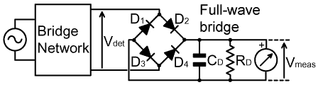
| This
circuit however has two disadvantages; one being that it has two diode
forward voltage drops in the path to the meter, so it is not so good
for crystal receivers and the other being that both output terminals of
the measuring bridge must always float with respect to either terminal
of the meter. The arrangement therefore creates problems in the matter
of where to connect the system ground for best isolation between input
and output, and is not usually a good choice. Despite the caveats, one advantage of the bridge rectifier is that the maximum inverse voltage for any of the diodes is only �2 times the RMS input voltage. The magnitude of the inverse voltage across D2 is is prevented from rising above Vdet�2 by the clamping action of D1 and vice versa. The same argument applies for D3 and D4.
|
Bi-phase rectifier
A full-wave detector which has only one diode forward voltage-drop in
the path to the meter, and is completely free from grounding problems,
is the bi-phase rectifier. This one of the best choices for crystal
detectors.
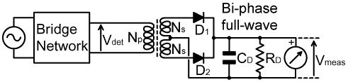
| By conducting on both half-cycles of Vdet, this circuit also halves the average diode current for a given output voltage and so reduces the diode forward voltage drop compared to that of a half-wave circuit. The only disadvantage is that it requires a centre-tapped coupling transformer. Care mush be taken in the construction of the coil. The two output coils should be as identical as possible. Also all windings must be winded in the same direction. The output voltage is given by the expression: Vmeas=Vdet�(�2)Ns/Np, neglecting transformer losses and diode forward voltage drop. Correct operation requires that the transformer has sufficient primary inductance not to load the bridge significantly at the lowest frequency of operation, and that the transformer is working within its pass-band. For HF radio frequency applications, the transformer can be wound on a small ferrite toroid or two-hole (binocular or 'pig-nose') core. Note incidentally, that if a transformer is used for the voltage splitting network (ratio arms) of the bridge, it is possible to combine this transformer with the bi-phase detector transformer by using the fact that the bridge is a linear reciprocal network; which results in the configuration shown below: |
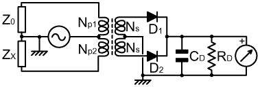
| This
circuit allows the unknown and reference impedances, the generator, and
the meter, all to have one terminal connected to ground. The
transformer will introduce some minor losses, but it will not introduce
non-linearity unless it is operated close to core saturation, which is
highly unlikely given the trivial power requirement of a 100mA meter. A
particular disadvantage of this configuration however, is that it
involves stuffing the ratio-arm transformer with a large amount of
wire, which makes it difficult to minimise stray capacitance between
the primary and secondary windings. The ratio-arm transformer must be
designed with great care, and in general it is best not to try to make
it perform additional functions. With regard to diode VRM, note that the bi-phase rectifier is simply two half-wave rectifiers feeding the same smoothing capacitor. Hence the inverse voltage rating for a diode must be at least 2�2 times the RMS voltage at the transformer output. As mentioned before, the bi-phase rectifier gives an improvement in linearity over the half-wave rectifier by dividing the rectifier current between two diodes; but as will be discussed next, the diode forward voltage drop varies logarithmically with current in such a way that the improvement will not be particularly large, and so the additional complexity may not be warranted. For the Omega receiver I have decided to go for the bi-phase rectifier topology, based on it's obvious advantages over the other topologies. The second generation of the receiver may use a FET detector, but I first have to make a better research on this type of detector. So, for the time being, and to satisfy more classical set readers I will end up to this topology. |
| After
deciding the detector topology I have to decide the type of diodes that
I will use. Let me tell a few words about diode forward voltage drop
and make a comparison between some diode types that can be used in a
crystal receiver. All of the diode detectors described above have at least one diode forward voltage-drop in the path to the measuring device. The diode forward voltage drop, Vf, varies approximately in proportion to the logarithm of the current, If, passing through the diode, and also depends on the temperature of the diode junction. For many types of diode, this behavior is described to a good approximation by a modified form of the Ebers-Moll equation:
where k is
Boltzmann's constant (1.380662�10 |
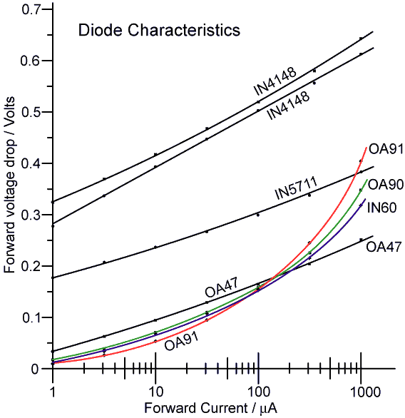
| The
1N4148 is a silicon P-N junction diode. The 1N5711 is a silicon
Schottky diode. The OA47 is an archaic germanium gold-bonded diode, and
the rest are germanium point-contact diodes. Two 1N4148 diodes from
different manufacturers were measured merely to illustrate the point
that silicon P-N diodes have the highest forward voltage drop and are
therefore a poor choice for low voltage detectors. The 1N5711 curve is
the average of results from four diodes, all from the same batch, which
had practically identical characteristics. The OA47 curve is the
average for four diodes from two manufacturers, all having similar
characteristics. The OA90, OA91, and 1N60 curves are from single
examples, and are therefore not necessarily representative of the type.
All data were recorded at an ambient temperature of 21�C. The data indicate that the IN4148, the 1N5711, and the OA47, all obey a logarithmic V/I relationship rather well, whereas the germanium point-contact characteristics show considerable curvature due to high internal resistance. With regard to the forward drop however, the germanium diodes are all superior to the IN5711 in the 1-100mA range, and the preference for the latter may merely reflect the fact that many semiconductor manufacturers can no longer fabricate germanium. Silicon Schottky diodes, such as the 1N5711 and 1N6263, being essentially UHF devices, have better high-frequency performance than germanium diodes, but germanium diodes work well at VHF and are therefore perfectly adequate for HF applications. Among the germanium diodes, there is little difference between the gold-bonded and standard varieties in the 1 to 100mA range, but the OA47 is the best choice for currents up to 1mA. We should observe however, that detector diodes only conduct on the peaks of the applied waveform, and so the instantaneous current is much higher than the average current, the difference being about an order of magnitude. Therefore, in selecting diodes for average currents in the region of 1 - 100mA, we should consider the steady-state voltage drop in the region 10mA - 1mA; in which case the germanium gold-bonded diode offers the lowest forward-drop without contest. Note however, that one of the consequences of the Ebers-Moll equation is that low forward voltage-drop is associated with high reverse leakage current. If reverse leakage is an issue, then silicon Schottky diodes are to be preferred. To put this issue in perspective however, the reverse leakage current of an OA47 diode was measured as follows: |
|
Vr /Volts |
1.0 |
2.0 |
3.0 |
5.0 |
10.0 |
15.0 |
20.0 |
|
Ir /mA |
1.1 |
1.3 |
1.4 |
2.1 |
4.1 |
6.3 |
8.8 |
| The leakage current is approximately linear in the 5-20V range and may be modelled by assuming a resistor of about 2MW in parallel with the diode. Such a defect has little effect on the operation of a detector loaded with a 10-100KW resistor. Some final points in favour of the silicon Schottky diodes however, are that germanium diodes show a wider spread of characteristics, and that the OA47 is obsolescent. Hence the Schottky diodes are definitely preferable in applications requiring diode matching, precise calibration, or availability through normal commercial channels. The 1N5711 in particular also, has a very high reverse breakdown voltage for a device of its class, its Vr max of 70V making it suitable for half-wave detectors of up to 24.7V DC ouput. An OA47 half-wave detector has a maximum DC output of 10.6V if Vr max is not to be exceeded. |
| Detector diode data: |
| Type | Description |
Vr max |
If max |
If av |
Typ Vf @ If |
Typ Ir @ Vr |
||
|
/ V |
/ mA |
/ mA |
/ V |
|||||
| 1N5711 | Si Schottky (2.0pF) |
70 |
- |
- |
0.41* |
1 |
0.2 |
50 |
| 1N5712 | Si Schottky (1.2pF) |
20 |
- |
- |
0.55* |
1 |
0.15 |
16 |
| AA119 | Ge point contact |
45 |
100 |
35 |
2.6 |
30 |
170 |
45 |
| AAY30 | Ge Au-bonded. High speed |
30 |
400 |
- |
0.88 |
150 |
8.0 |
30 |
| AAY32 | Ge Au-bonded. High speed |
30 |
150 |
- |
0.60* |
30 |
11 |
30 |
| AAY33 | Ge Au-bonded. High speed |
12 |
240 |
- |
0.5* |
30 |
15 |
12 |
| AAZ15 | Ge Au-bonded. High voltage |
100 |
250 |
- |
0.8 |
250 |
16 |
100 |
| AAZ17 | Ge Au-bonded. Gen.purpose |
75 |
250 |
- |
0.8 |
250 |
16 |
75 |
| BAT81 | Si Schottky (1.6pF) |
40 |
30 |
- |
0.33 |
0.1 |
0.2 |
30 |
| BAT82 |
50 |
|||||||
| BAT83 |
60 |
|||||||
| OA47 | Ge Au-bonded. Gen.purpose |
30 |
150 |
- |
0.54 |
30 |
10 |
30 |
| OA90 | Ge point contact "diode"?** |
30 |
45 |
10 |
2.0 |
30 |
300 |
30 |
| OA91 | Ge point contact |
115 |
150 |
50 |
2.1 |
30 |
75 |
100 |
| OA95 | Ge point contact |
115 |
150 |
50 |
1.85 |
30 |
80 |
100 |
| *
max. ** a very non-linear resistor pretending to be a diode - best avoided! |
For the Omega
receiver I have decided to go for the OA47 diode, based on it's obvious
advantages over the other diodes. The second generation of the receiver
may use a FET detector, but I first have to make a better research on
this type of detector. So, for the time being, and to satisfy more
classical set readers I will end up to this type of diode.
| Back
Diodes: One further rectifying device which we should mention in passing is the backward diode or 'back-diode'. This is a special type of tunnel diode (Esaki diode), which has an extremely low forward voltage drop: in the region of 90mV for 10mA forward current. Unfortunately however, there is no get-out-of-jail-free card as far as the Ebers-Moll equation is concerned: the back diode has an extremely low reverse breakdown voltage, and a leakage of around 1mA for a mere 500mV of reverse bias. The back diode can therefore only be used in extremely low-impedance low-voltage circuits, which comprehensively defeats any advantage it might have had for the construction of linear detectors. |
Below I would like to mention two useful things about diodes. The detected voltage as function of the input voltage and the detector diode input impedance
| Detected
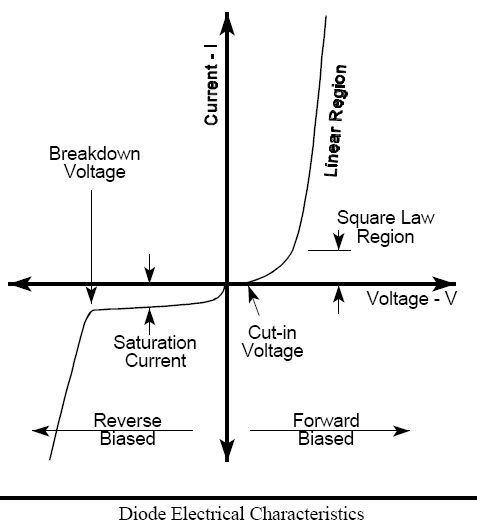
voltage as function of the input voltage If we rectify a RF signal with a diode we can distinguish two situations. Situation 1: Rectifying in the linear region If the input voltage is high enough (well above the voltage drop of the diode at 1 mA), the output voltage of the diode will be about proportional to the input voltage. So double input voltage, gives about double output voltage. The output voltage is almost equal to the peak value of the input voltage. The power losses in the diode are in this region very low compared to the rectified power. Situation 2: Recifying in the square law region If the input voltage is low, lower then the voltage drop of the diode (at 1 mA) then the situation is completely different. The input of the diode behaves for the RF signal like a resistor with value RD. The output of the diode behaves like a DC voltage source in series with a resistor, the value of this resistor is also equal to RD. The value of the DC voltage source is square law related to the amplitude of the RF input signal. So double input voltage, gives 4 times as much detected DC voltage at the output In the square law region the output voltage of the diode will be much lower then the input voltage, the diode gives much power loss between input and output. The lower the input voltage, the higher the losses. The higher the input voltage, the lower the diode losses. When further increasing the diode input voltage, we gradually come into the linear detection region. When receiving weak stations, detection takes place in the square law region. Between the linear and square law region, there is a region not linear, and not square law but somewhere in between. |
| Detector
diode input impedance A point to which we have so-far only alluded, is that the load presented by the detector has a significant effect on the operation of some types of bridge. We must therefore always keep the detector input impedance in mind when investigating bridge behaviour, and in order to do so we need to have an idea of its value. This is a peculiar problem in the case of a diode detector, because the diode does not obey Ohm's law; and so the input resistance varies during the course of each cycle of the applied voltage. For the most part however, it is sufficient to have an average picture of the detector input impedance, and this can be obtained by considering the power delivered to the detector load resistor RD. |
| In
the first instance, we can consider the power delivered to RD in the limit that the peak value of
the applied voltage Vdet is
very large in comparison to the diode forward voltage drop Vf. In this case, the detector output
voltage is: Vmeas = Vdet �2 and the power delivered to the load resistor is: Pdet = Vmeas� / RD |
|
| Now,
all of this power must come from the bridge output. Therefore, if we
define the detector input resistance as Rdet,
we have: Pdet = Vdet� / Rdet = Vmeas� / RD and using equation (Vmeas = Vdet �2) gives: Vdet� / Rdet = (Vdet �2)� / RD i.e., 1 / Rdet = 2 / RD i.e.,
Thus the
limiting input resistance of a simple detector is equal to
half the detector load resistance. We can understand this
point by thinking of the detector as a kind of voltage transformer. The
RMS average of a DC signal is the same as its ordinary average, and so
in the process of converting from AC to DC, the RMS level has been
transformed-up by a factor of �2. Thus the detector is a 1:�2 voltage
transformer, and hence a 1:(�2)�, i.e., 1:2 impedance transformer.
Thus the
voltage-doubler is a limiting 1:8 impedance transformer. Consequently,
it has a much lower input resistance in comparison to a non-multiplying
detector for a given value of detector load. The difference is such
that advantage of increased output voltage can easily be lost as a
result of loading of the driving circuit. |
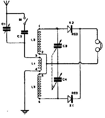
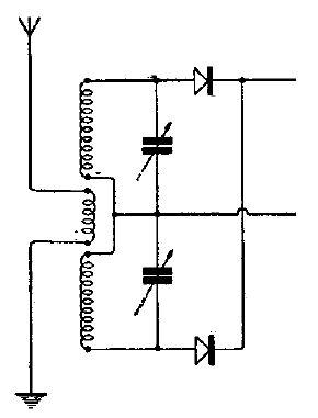
I believe I gave you a feeling about the issues related to the detector. So let me summarize the construction of the Omega receiver at this point using the following schematic.
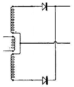
The input RF signal is connected to the center coil and the audio signal is coming out of the center tap and the positive of the two diodes. This one works ok if we are referring to a single frequency rectification like for example 50 Hz mains. In radio frequencies multiple signals appear simultaneously to the antenna and thus to the center coil and so we have to have a way of selecting the desired signal from the many unwanted ones. This can be done by creating tuned circuits with the use of a variable capacitor that is connected parallel to the output coil. Here we have a symmetrical configuration so we need two of these circuits and thus two capacitors. As I said earlier, care must be taken when constructing the coil. The symmetrical circuits must be as matched as possible for the circuit to work efficiently. This is the price you have to pay for the greater power gain. In the input center coil you must connect the antenna and the earth. Now the Omega receiver will look somehow like this:
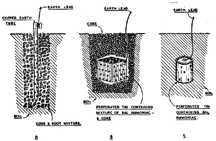
Before I carry on I think it is time to present a few things about earthing. In crystal receivers earthing is as important as the antenna. The figures below show three good earthing techniques.
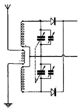
Now
that I have shown you the earthing bit let's go back in our Omega
receiver. For the tuned circuits to be matched in a symmetrical circuit
the tuning must be made equal to each of them. An easy way to achieve
this is to use a dual gang variable capacitor. Each gang is connected
to one of the two secondary coils, so when you rotate the capacitor you
tune the symmetrical circuits equally. This has the advantage that the
user does not need to tune two capacitors each time but just one
double. This is fine in theory but in practice there is no perfectly
matched capacitor. Even the dual gang types have small differences in
the capacitance of each of their sections. To overcome this problem we
can add a small variable capacitor in parallel with each main tuning
capacitor. The total capacity of each gang will then be the capacity of
the main tuning plus the capacity of the small variable capacitor. By
tuning the small variables respectively, and measuring the total
capacity of each gang of the big variable capacitor, you can create a
matched dual gang capacitor.
For this circuit, measuring and matching your capacitor is not actually
needed. This is because it is not only the capacitor that affects the
frequency but also the coil. If the coil of the one section has a bit
different inductance than the coil of the other section then the
capacitor of the first section must have a bit different capacitance
than the capacitor in the second section in order for the two tuned
circuits to be equal. The ideal case would be to have perfectly matched
coils. In that case we would need a perfectly matched capacitor. But
the fact is that homemade coils are difficult to be made perfectly
matched. Thus, the addition of a small parallel variable capacitor
offers the advantage of perfectly matching the two sections of the
circuit. The schematic of the Omega receiver up to this point, can be
seen below.
Tuning such a circuit is not as difficult as it seems. First turn the two small variables at about a half of their capacity. Then tune to a frequency stable loud station using the dual gang variable. Then re-tune the two small variables one after the other, in order to achieve the loudest output signal. The less the bandwidth of the incoming signal, the more accurate you can match the two sections.
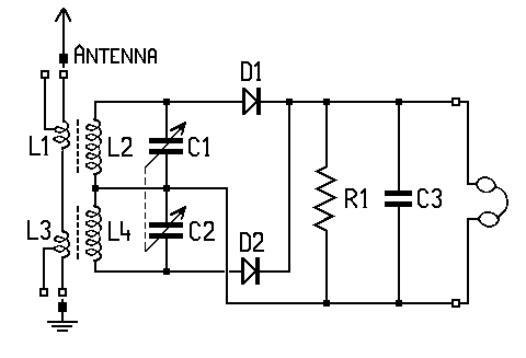
The heart of the omega receiver circuit is fine up to this point. It should be a very sensitive classical crystal receiver for all the reasons described in the previous sections. But the selectivity is not great yet. As I said earlier, the two main performance issues in crystal receivers are sensitivity and selectivity. For the Omega receiver I do not want to degrade sensitivity for the benefit of selectivity and vice versa. A form of circuit to improve selectivity must be used. There are several circuits that can do that, each one can do it better or worst than the others and each one has advantages and disadvantages. At the beginning of the page I have shown many circuits that are using tuned circuits of coils and capacitors to improve selectivity. Some of them are using band pass filters. To my point of view band pass filters are the most suitable for good selectivity. They perform well and that is why they are extensively used in microwaves where the applications are critical. They are also very straight forward. They allow only a certain part of the band to pass into the next stage. I have read that band pass filters have some insertion loss, but I think this can be compensated with the detector type that I have used. I am telling that because almost all the band pass circuits that I have shown at the start of the page use just a single diode detector, yet they claim that they perform very well. A band pass filter is composed of two parts. The low pass filter, which cuts off the higher frequencies and the high pass filter, which cuts off the lower frequencies. The two parts are coupled together incuctively or capacitively. By using this combination of low pass and high pass filter, a band pass filter can be made. The next picture shows such a band pass filter, in the red square.
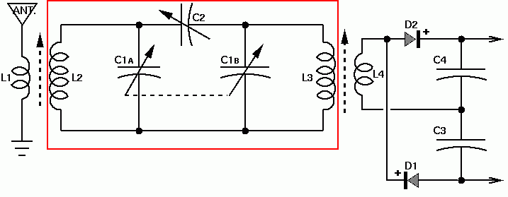
Note,
there must be an error in the above circuit, although I haven't test it
at the time I am writing these lines. All the band pass filters that I
have seen connect their bottom side to the ground. Based on this, I
would then connect the L2, C1A, C1B and L3 to the ground, at their
bottom end, but this is something I have to test first. The circuit is
called double tuned band pass filter because it uses two tune
capacitors. It is also capacitively coubled using another variable
capacitor.
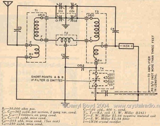
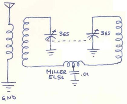
The circuit below comes from an old miller set. It does not use
capacitive coupling but it connects the two parts of the filter using a
third coil. I have found that this coil provides negative mutual
inductance between the two tuned circuits to maintain a constant
bandwidth across the entire tuning range. however I have also found
that in the capacitor coupling circuit above, the variable capacitor C2
should be adjusted for the best selectivity and volume over the entire
broadcast band. So I think that these two circuits have about the same
performance.
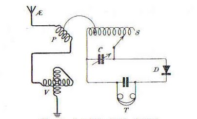
The capacitive coupling circuit is extensively used today by radio amateurs in modern sets because it's performance is good and it is easy to construct. Besides, I cannot find more information about winding homebrew coils for the second circuit, so I have decided to go for the first approach. However, since it uses a dual gang capacitor to tune the two filter parts, the addition of a small variable capacitor in parallel with each main tuning capacitor is mandatory for the reasons described previously. The filter will be inductively coupled to the detector section and to the antenna. Based on the above considerations, the final circuit up to this point for the Omega receiver can be summarized below.
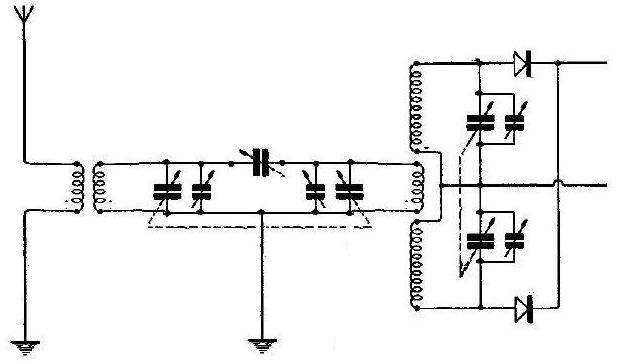
Now, do not be scared about the many variable capacitors. The actual tuning capacitors (knobs) are three. This circuit seems quite selective and complete, but there is a glitch. Generally, the more components you have in such a passive circuit, the more losses you have. If you connect just a diode at the antenna using no coils and capacitors, these losses are minimum and they are determined by the losses of the diode, the antenna cable and the losses of the headphones. But the selectivity in this case is very poor and it is only determined by the resonance of the antenna itself. For a successive receiver you have to find a compromise between selectivity and losses or as usually mentioned, selectivity and sensitivity. This is an interesting topic that needs a lot of experimenting and constructing the actual circuits, rather than investigate them in theory.