Broadband reflection coefficient bridge
by SV3ORA
The reflection coefficient bridge is a very useful lab instrument. It can be used in lots of measurements to verify the theoretical calculations. Sometimes, it is not easy at all to do these calculations and the only way is to perform measurements directly to the actual circuit, to verify it's performance. This is where the reflection coefficient bridge comes in. Before building this bridge and without any other special lab equipment, I was really blind when trying do things like matching the impedance of two circuit stages.
The goal is to build a very broadband reflection coefficient bridge. This eliminates the need for having multiple instruments to cover a wide range of frequencies. This also means that the bridge circuit must not use any kind of resonant circuits. Also, to cover a portion of the microwave spectrum, is has to be made using SMD components, the PCB must be miniaturized and good quality connectors have to be employed. Another requirement is that this instrument must be lightweight, rugged and require no power to operate, other than the power that comes from the RF signal itself (passive). When testing for example HF antennas, you do not want to find yourself in a situation of hanging on a 30m tower and carrying heavy equipment with you. This also applies to VHF/UHF/SHF antenna arrays, where each individual antenna in the array needs to be tested.
Electronic design
Reflection coefficient bridges are broadband RF comparators. These devices develop a DC potential with respect to ground which is proportional to the degree of imbalance in the arms of the bridge circuit. With this in mind, the next circuit was developed. The amount of impedance difference between Z1 and Z2 ports, is indicated by a positive potential at the DC out port. The most positive the voltage at this port, the greater the imbalance and the greater the mismatch. The circuit also includes an auxiliary monitor out port, which is essentially a detector that rectifies the incoming RF signal and monitors its power level. The greater the DC voltage at this port, the higher the incoming RF signal level.
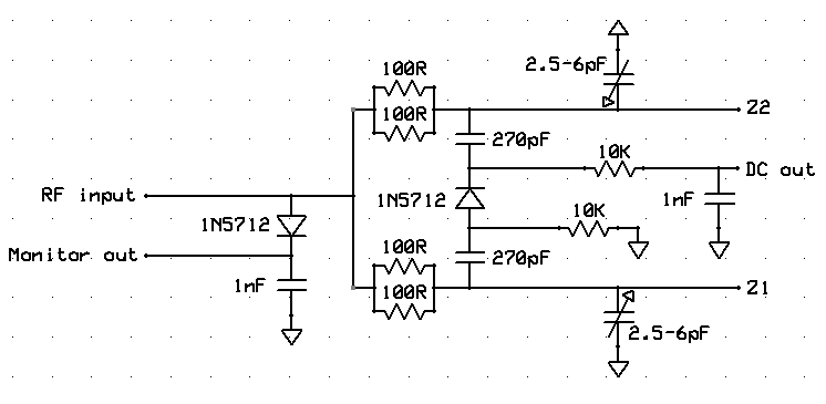
The construction of the circuit is fairly straight forward. For the diodes, I used the 1N5712 type. Although better microwave diodes exist, the 1N5712 has only 1.2pf of junction capacitance, it is widely available and very cheap. For the variable capacitors, I used 2.5-6pf SMD variable trimmers. Each of the two 50R resistors, was made using two 100R in parallel, as these were easier to obtain. Additionally, this allows for more power handling and greater precision of the total resistance value. The PCB is 0.8mm FR4 (not critical at all) dual sided and the back side is full of copper acting as the ground plain.
ExpressPCB
PCB file
PCB PDF file
ExpressPCB schematic file
Mechanical design
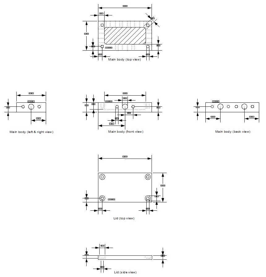
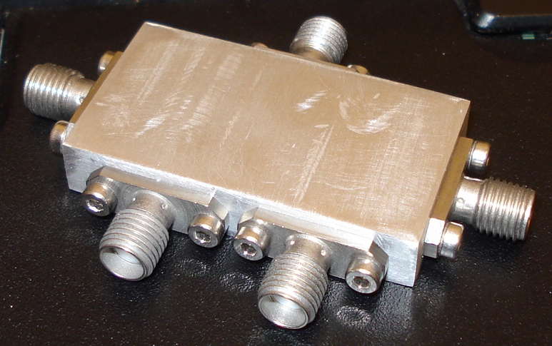
A well made instrument must have good electrical but also mechanical properties. Since the bridge will be carried and handled in the field, it's mechanical rigidity and ease of use is important as well. The circuit is quite small, so a suitable enclosure can be milled from a piece of aluminum block, if a mill is available. The dimensions and the overall mechanical design of the enclosure are presented below.
Vectorengineer CAD file
PDF file
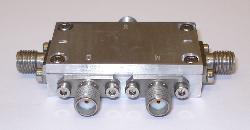
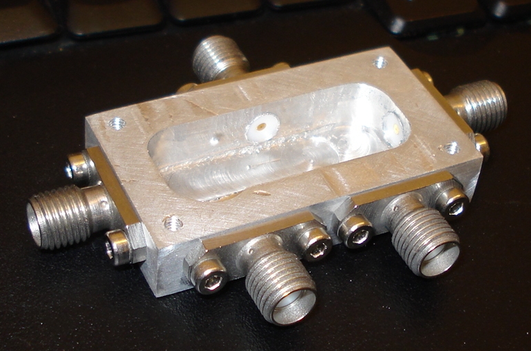
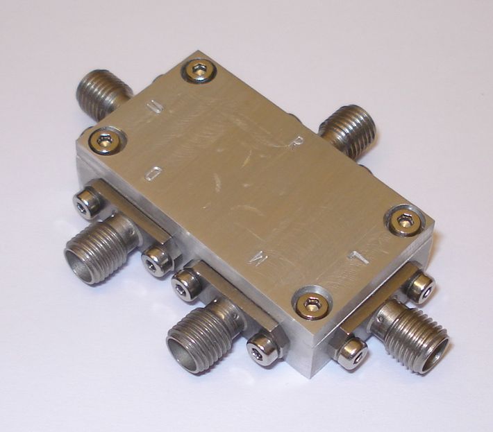
The SMA connectors that are used, are all stainless steel, teflon insulated types, that have a cut-off frequency well into the microwave region. You may notice that the monitor out and dc out ports use SMA connectors as well, while this is not really necessary. Alternatively, feed through screw-type capacitors could be used, as only DC is of interest at these ports. However, the use of coaxial connectors for these ports, has the advantage of being able to make quick connections without the need for a soldering iron or unsteady crocodile clips. Additionally, the use of the same type of connectors, as that used for the other ports (SMA), allows for only one interconnect cable type to be used for all ports, which is cheaper and more convenient in the field. The shunt capacitors are placed very close to these connectors in the PCB layout anyway.
Implementation
Implementation of the design, begins with the etching of the PCB and the placement of the components onto it. Use your favorite etching process and carefully etch the PCB. A thin 0.8mm PCB will fit nicely inside the enclosure, but its thickness does not really affect circuit operation. Whereas SMD components are used, their sizes have been chosen not to be very small, so that they can be easily soldered with a standard fine tip soldering iron. An SMD rework station is really not required to build the circuit.
After completion of the PCB, the enclosure has to be made. Start with a small block of aluminum, with the closest dimensions you can find to the proposed mechanical design, so that you do not have to remove a lot of material from the block (which is time consuming).

Place a suitable size end-mill to the rotating head and square the aluminum block to the dimensions of the design, using the front and the sides of the end-mill.
The next procedure is to mill a pocket into the aluminum block. Take care not to
lower the end-mill too much, to avoid drilling the enclosure all the way down to
the other side. After the pocket is made, carefully drill the holes for the SMA
connectors and the lid. Then use a screw maker tool of the appropriate size, to
form the screws for the SMA connectors and the lid. If you wish, you may use a
sand paper to smooth the enclosure surface even more. Finally, screw the SMA
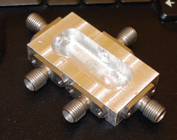
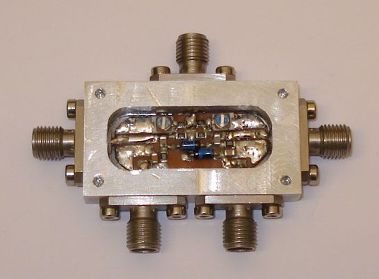
connectors in place. The final enclosure should look like the pictures below.
To fit the PCB inside the enclosure, you may have to cut it's corners so that they are diagonal. The amount of PCB that needs to be cut, depends on the diameter of your end-mill. It is recommended to cut the PCB before you mount the components onto it, to avoid damaging them.
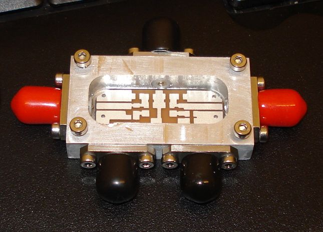
The end result, should look like the picture below. Note that the diodes in the picture, are shown connected in the opposite direction from that in the PCB layout. It was an initial test to determine if negative voltages can be employed out of the measurement ports and it worked indeed. The PCB layout is the positive version, which has been finally used, since positive voltages are more convenient.
To reduce the overall thickness of the enclosure, I did not include screws to screw the PCB GND to the case, so I used a bit of metallic sponge (metallic scotch brite) between the bottom of the PCB (GND) and the enclosure, to fully ground the PCB.
The enclosure lid, is made using the same procedure described above. The holes to support the screws of the lid are made bigger on the top side, so that the screw heads can dive into the aluminum lid.
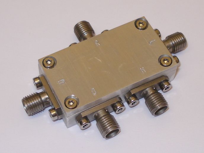
Letters have been punched at each port to define it, using a stainless steel letter punch kit. R is the RF port, L is the 50 ohm reference load Z1, M is the monitor out, D is the DC out and U is Z2, the unknown impedance device under test.
Calibration
To calibrate the device, a wideband signal generator is needed. Alternatively a VHF/UHF or triband radio amateur transceiver could be used, with a suitable attenuator at the output. The signal generator output must be connected to the R port and two matched 50R loads to the L and U ports. The D port, is connected to the 1Mohm port of an oscilloscope, or a sensitive high impedance volt meter. The signal generator must be tuned to the highest possible frequency.
To balance the bridge, switch on the signal generator and slowly tune the two variable capacitors with a non-magnetic screwdriver, whereas monitoring the voltage at the D port. The variable capacitors are there to compensate for differences in input and output capacitance due to construction differences and component tolerances. When the bridge is perfectly balanced, the voltage at the D port must be the minimum possible. Try also different frequencies near the top frequency limit of your signal generator and repeat the setting if required. In general, when balanced correctly at higher frequencies, switching to much lower frequencies should require no further tuning.
The worst case scenario in the prototype, was at 470MHz, which measured 5mV at D port, but this was due to the initial unmatched commercial loads used at Z1 and Z2. At 530MHz, using the same loads, that voltage was zero. When connecting matched loads the worst case scenario dropped at only 2mV. The bridge should work down to quite low frequencies, the only thing that happens is it becomes a little less sensitive as the reactance of the 270pF capacitors becomes significant.
To quickly test that the circuit works, remove the 50 ohm load from the U port and connect different resistors from the central SMA conductor of this port, to the ground. The voltage at the D port, should be higher if a different value resistor, other than 50 ohm, is connected. The greater the difference of this resistor from the 50 ohm reference load, the higher the voltage at the D port.
Measurements
Return loss
Return loss can be measured by taking the D port voltage with U terminated, divided by the D port voltage without any U termination. That value is then feed into the following formula: Return Loss (dB) = -20 * log10(p) where p is the value you determined from above measurement.
Note that L port should be terminated with a non-inductive 50 ohm reference load.
If a computer program is used, the calculation can be done more easily. Here is a sample program in Perl:
    $p = $DC_voltage_terminated / $DC_voltage_not_terminated);
    $rtrnloss_db = -20 * log10($p);
    $SWR = (1 + $p) / (1 - $p);

    Example: Unterminated voltage is 2.0 Volts
             Terminated voltage is 0.8 Volts
             Then the return loss is 7.96 dB or a SWR of 2.33

A large positive return loss, indicates the reflected power is small relative to the incident power,
which indicates good impedance match from source to load.
Insertion loss
It is possible to use the return loss bridge to determine the insertion loss of coaxial cable systems. In coaxial cables, the insertion loss is comprised of resistive losses (skin effect) and dielectric losses. Each of these parameters increases with frequency. The insertion loss of a cable system is determined by observing the reflections from an open (or shorted) output.
Cable Insertion Loss Measurement Example:
- Perform the initial return loss bridge calibration. That is, measure the D port voltage, at the operating frequency, of a unterminated bridge.
- Open (or short) one end of the the cable you wish to test.
- Connect the other end of the cable to the return loss bridge's U port.
- Determine the SWR using the procedure described above.
- Refer to the table below, to correlate SWR to insertion losses.
Cable Insertion Loss Vs. SWR table:Cable Insertion Loss = -10 * log10 * (SWR - 1 / SWR + 1)
SWR Insertion Loss (dB)
1.05 16.3
1.1 13.2
1.2 10.4
1.3 8.7
1.4 7.8
1.5 7.0
1.6 6.4
1.7 5.9
1.8 5.5
1.9 5.1
2.0 4.8
2.5 3.7
3.0 3.0
3.5 2.6
4.0 2.2
4.5 1.9
5.0 1.8
6.0 1.5
7.0 1.2
8.0 1.1
9.0 0.96
10.0 0.88
20.0 0.43
30.0 0.29
40.0 0.23
Structural Return Loss
It is also possible to use the return loss bridge to determine the structural return loss of coaxial cable systems. Structural return loss is basically a measure of the quality of a cable. In coaxial cables, structural return loss is caused by any imperfections in the overall cable system. Reflections will occur from variations in the cable's diameter, dielectric imperfections, sharp bends, center conductor misplacement, stupid people installing connectors, etc. These reflections prevent a certain portion of the forward RF power from ever reaching the antenna system or load.
Cable Structural Return Loss Measurement Example:
Structural Return Loss Vs. SWR table:
- Perform the initial return loss bridge calibration. That is, measure the DC output voltage, at the operating frequency, of a unterminated bridge.
- Terminate one end of the the cable you wish to test with a load matching the cable's characteristic impedance, 50-ohms usually.
- Connect the other end of the cable to the return loss bridge's U port.
- Determine the SWR using the procedure described above.
- Refer to the table below, to read structural return loss in terms of SWR.
Structural Return Loss = 20 * log10 * (Voltage Reflected / Voltage Reference)


Vreflected / Vreference		Structrual Return Loss (dB)	SWR

1.12				1				17.40
1.26				2				8.72
1.413				3				5.85
1.585				4				4.42
1.778				5				3.57
1.995				6				3.00
2.239				7				2.62
2.512				8				2.32
2.818				9				2.10
3.162				10				1.92
3.584				11				1.78
3.981				12				1.67
4.467				13				1.58
5.012				14				1.50
5.623				15				1.43
6.310				16				1.38
7.079				17				1.33
7.943				18				1.29
8.931				19				1.25
10.00				20				1.22
11.22				21				1.20
12.59				22				1.17
14.13				23				1.15
15.85				24				1.13
17.78				25				1.12
19.95				26				1.11
22.39				27				1.09
25.12				28				1.08
28.18				29				1.07
31.62				30				1.06
35.48				31				1.058
39.81				32				1.051
44.67				33				1.046
50.12				34				1.041
56.23				35				1.036
63.10				36				1.032
70.79				37				1.029
79.43				38				1.026
Also, see the next useful graph for SWR to Return Losses:Return
Loss Reflected Transmiss.
VSWR (dB) Power (%) Loss (dB)
---- ---- --------- ---------
1.00 oo 0.000 0.0000
1.01 46.1 0.005 0.0002
1.02 40.1 0.010 0.0005
1.03 36.6 0.022 0.0011
1.04 34.1 0.040 0.0018
1.05 32.3 0.060 0.0028
1.06 30.7 0.082 0.0039
1.07 29.4 0.116 0.0051
1.08 28.3 0.144 0.0066
1.09 27.3 0.184 0.0083
1.10 26.4 0.228 0.0100
1.11 25.6 0.276 0.0118
1.12 24.9 0.324 0.0139
1.13 24.3 0.375 0.0160
1.14 23.7 0.426 0.0185
1.15 23.1 0.488 0.0205
1.16 22.6 0.550 0.0235
1.17 22.1 0.615 0.0260
1.18 21.6 0.682 0.0285
1.19 21.2 0.750 0.0318
1.20 20.8 0.816 0.0353
1.21 20.4 0.90 0.0391
1.22 20.1 0.98 0.0426
1.23 19.7 1.08 0.0455
1.24 19.4 1.15 0.049
1.25 19.1 1.23 0.053
1.26 18.8 1.34 0.056
1.27 18.5 1.43 0.060
1.28 18.2 1.52 0.064
1.29 17.9 1.62 0.068
1.30 17.7 1.71 0.073
1.31 17.4 1.81 0.078
1.32 17.2 1.91 0.083
1.33 17.0 2.02 0.087
1.34 16.8 2.13 0.092
1.35 16.5 2.23 0.096
1.36 16.3 2.33 0.101
1.37 16.1 2.44 0.106
1.38 15.9 2.55 0.112
1.39 15.7 2.67 0.118
1.40 15.6 2.78 0.122
1.41 15.4 2.90 0.126
1.42 15.2 3.03 0.132
1.43 15.0 3.14 0.137
1.44 14.9 3.28 0.142
1.45 14.7 3.38 0.147
1.46 14.6 3.50 0.152
1.47 14.5 3.62 0.157
1.48 14.3 3.74 0.164
1.49 14.2 3.87 0.172
1.50 14.0 4.00 0.18
1.55 13.3 4.80 0.21
1.60 12.6 5.50 0.20
1.65 12.2 6.20 0.27
1.70 11.7 6.80 0.31
1.75 11.3 7.40 0.34
1.80 10.9 8.20 0.37
1.85 10.5 8.90 0.40
1.90 10.2 9.60 0.44
1.95 9.8 10.2 0.47
2.00 9.5 11.0 0.50
2.10 9.0 12.4 0.57
2.20 8.6 13.8 0.65
2.30 8.2 15.3 0.73
2.40 7.7 16.6 0.80
2.50 7.3 18.0 0.88
2.60 7.0 19.5 0.95
2.70 6.7 20.8 1.03
2.80 6.5 22.3 1.10
2.90 6.2 23.7 1.17
3.00 6.0 24.9 1.25
3.50 5.1 31.0 1.61
4.00 4.4 36.0 1.93
4.50 3.9 40.6 2.27
5.00 3.5 44.4 2.56
6.00 2.9 50.8 3.08
Applications
Return loss bridges are useful in measuring VSWR, or return loss of filters, mixers, antennas and amplifiers. They can also be used for load matching. Since there are no resonant circuits in the prototype, it's frequency range is very broadband, so wide sweep testing of all the above devices is possible. The bridges may also be used for coupling two generators for intermodulation testing or power splitting for leveling systems. They can also be used as signal combiners to combine two inputs to a single output. In this case, the U port is usually the combined port, with the other two ports as inputs (not verified in the prototype). Isolation between the two input ports of the bridge must be measured and considered too. Another factor to consider is the directivity of the bridge. Such specific factors have not yet determined in the prototype.
Although the bridge prototype has been built for 50 ohm systems, matching to other impedances can be accomplished by comparing the amount of imbalance with a known non-50 ohm load. The amount of error voltage should always be the same when the error is the same. For example measuring a supposed 200 ohm loop antenna to determine if it's impedance is really 200 ohm in a specific frequency, can be done this way:
Connect the reference 50 ohm load at the L port.
Short U port with a 200 ohm resistor.
Read the voltage at the D port and zero the meter.
Remove the 200 ohm resistor and connect the antenna to measure in place.
If the impedance of the antenna is 200 ohms at this specific frequency, then a zero reading will be noticed on the meter.
Note that the antenna impedance will vary, as the frequency that is feeding it changes. For example, a 50 ohms antenna should be 50 ohms at it's resonant frequency, but will go above or below that, as you move away from this frequency. Antennas are rarely as specified, for that very reason. When the manufacturer quotes 50 ohms, it will only be at one frequency and in the case of wideband antennas (TV antennas for example) it is quite normal for it to be widely off impedance at band edges. In a receiver antenna, that doesn't matter too much but in a transmitting antenna, you can see why an impedance matching network is usually employed, to maximize the radiation at the desired frequency.
Important measurement notes
When balancing the bridge
Make sure the loads connected at L and U ports are as identical as possible. Also make sure these loads connect with the same type and model of adaptors to the bridge. I used SMA M-M adaptors to connect two matched loads to the bridge when calibrating. When measuring, make sure you leave the same SMA adaptors connected to the bridge and connect the unknown device to port U, using the same SMA M-M adaptor. That way you ensure that you are not measuring the adaptor, but only the device under test.
When measuring the power (M port)
When measuring the return loss
Also note that: