The
"Super VFO"
As stable as a crystal!
by sv3ora
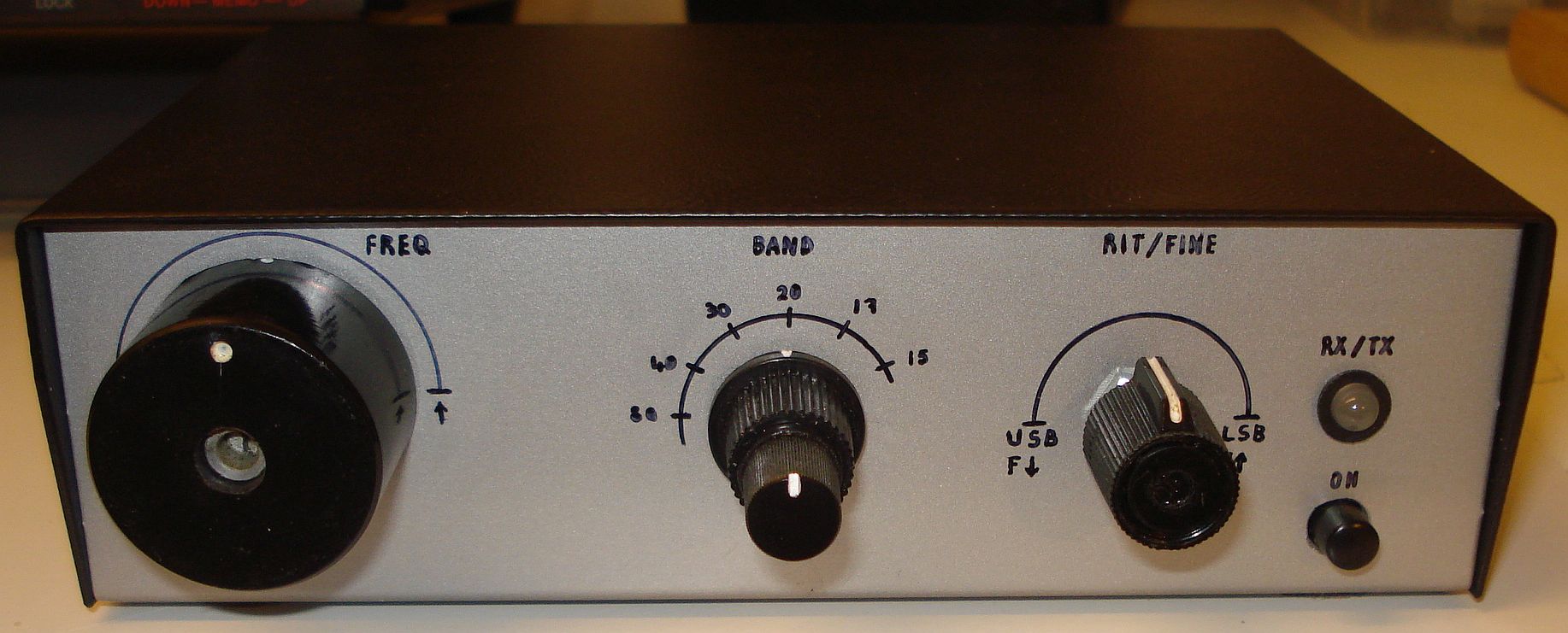
The front panel of the "Super VFO"
This "Super VFO" is a design of mine. It will give you rock-stable variable frequency operation at all HF bands and so it can be used reliably for your HF transceivers. I called it a "Super VFO" because of its features:
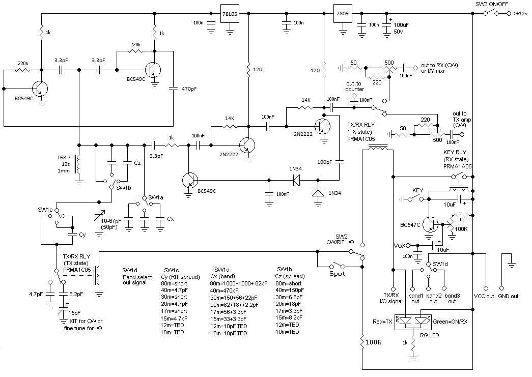
The deluxe version of the "Super VFO".
The full featured version of my "Super VFO" is shown above. This version includes all the features mentioned in the list at the beginning of this article. However, to better describe the operation of the core of the VFO, let's look at the simplistic bare-bones version of the VFO below.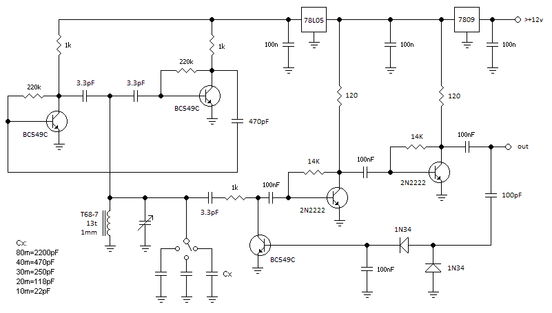
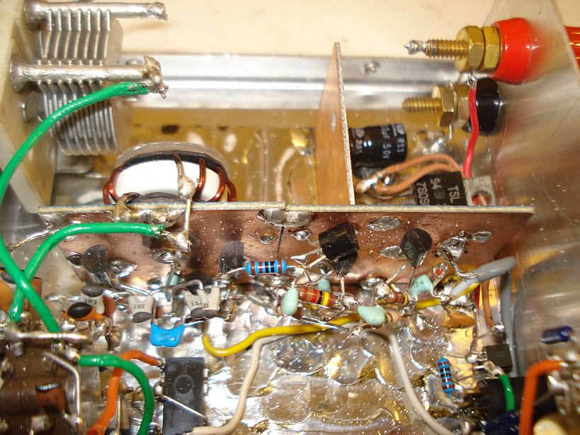

An overview of the internals of the finished "Super VFO".
It is important for the power supply to be able to provide a stable voltage to the VFO. This is accomplished by the use of two linear regulators. It could be made discrete, but linear regulators are very comon nowadays and I thought it would not worth the extra components needed for a discrete circuit. The 5V regulator can be the 78L05 (TO-92 package) or the standard 7805 (bigger package) but the 9V regulator must better be of the bigger package, as the buffer draws almost 60mA.
One of the most interesting things about this VFO is that for covering the whole HF (80m-10m) only a single untapped inductor is needed and a few range capacitors (which must be NP0). This makes it really easy to build, cheap and small-sized. Moreover, the frequency stability is more than adequate at all frequencies using this inductor alone. Build this inductor exactly as I did, with 13 turns of 1mm diameter enameled copper wire, evenly spaced around a T68-7 toroidal core. This will guarrantee you similar results as mine. Go ahead and experiment with other cores and coils if you like, but do not judge the frequency stability of your version of the VFO, based on your particular inductor, if it is not built as I describe. Keep the leads of the inductor short. You can also keep it firm by attaching it with a non-magnetic screw and a few pieces of plastic onto the PCB of the VFO, trying to keep it away from magnetic metals.
Close up
of the toroidal inductor, fitted in place.
From now on,
let's look at the deluxe version of the "Super VFO" to describe the
rest of its features. An important thing when building a general
purpose VFO that could be used in all shorts of circuits, is to be able
to vary it's output level accordingly, while keeping a nearly constant
output impedance. This can be done using switched attenuators, but for
simplicity a potentiometer is enough. In the configuration shown, the
output attenuators keep a relatively constant output impedance at all
attenuation settings near to 50 ohms.

The variable attenuators (potentiometers) for both TX and RX outputs.
The
frequency determining inductor of the VFO has been described earlier.
In the bare-bones version, a band switching NP0 type capacitor and a
variable capacitor are only used. However, to be able to operate the
VFO without the need for mechanical reduction drives and to make the
tuning convenient and within bands, a complex network of switching
capacitors (all NP0) is needed. SW1, is a quad-section 6-position
selector switch. Section SW1a is used for the band switching. Section
SW1b is used for the band spread, i.e. to make the tuning non-touchy.
SW1c takes care of the RIT/Fine-tune spread for each band. SW1d is used
for the band selection control signals. These signals can drive
external switched filters of other band-specific circuits if needed.
Note that for 80m, SW1b and
SW1c are shorted. Also on 30m,SW1c is shorted.
Because some
of the capacitors used in this network are very small, depending on the
parasitic capacitance of your own selector switch, you might not need
them, or you might need bigger values. This is all a trial and error,
but I provide you with starting values to begin with. You could use
variable trimmers instead of the lots of the fixed capacitors
combinations, but make sure these are all NP0.
Note that I have build the VFO for 6 bands because I only had a 6-position switch, but I have tested it and it can cover also the 12m and 10m with the same inductor. However, I could not test for the values of the band and spread capacitors in these bands, so this is up to you to determine it.

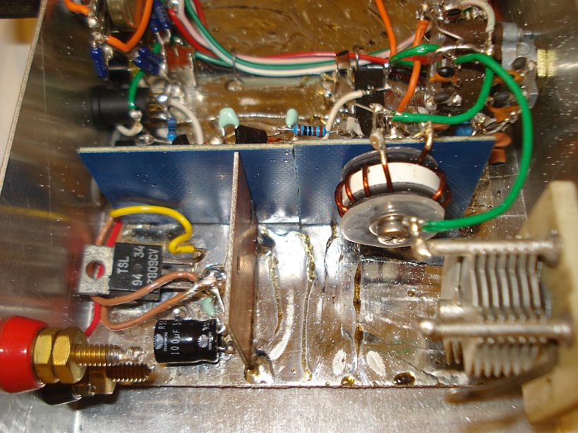
Close up of the selector switch and the tuning capacitors
On the DIN I/O connector used, apart from the band selection output signals, there is also a TX/RX I/O control signal available. This indicates the TX/RX state of the transceiver. The VFO switches this signal line to 12v to indicate to external circuits that TX is enabled. However other external circuits may also take over the switching of this line to 12v, to indicate the TX state of a transceiver. The VFO responds to this change as well and it automatically changes it's state. So this signal line is bi-directional. There is also a VCC line available on the DIN connector. This is optional and I left it there because I had a spare pin on the connector.
If it is to
control a transceiver from the computer, an embedded keyer needs to be
available. The Super VFO includes such a keyer which does several
things. In CW mode, it is used as a manual keyer, allowing the external
straight key to be connected to the ground. It also allows break-in
operation, meaning that the RX is automatically enabled after any
key-up. In CW and I/Q mode, it is also used as a VOX, allowing any
audio signal from the PC sound card to key the VFO. Whether in CW or in
I/Q mode, the keyer switches the TX/RX indicator and controls the TX/RX
control line on the DIN connector. However, the keyer is not controlled
by external TX/RX I/O control signals.
The keyer
works in a totally different way than the clasic voltage doubler and
transistor circuits. Here, the transistor works as an AF amplifier,
amplifying audio out of the sound card without rectifying it, so that
to make the circuit really sensitive in a single stage. The 100k
trimmer resistor must be set so that the relay is switched off, just
before it starts to switch on. This is not used as a sensitivity
control, it is used as bias setting for the transistor. The sensitivity
is controlled by your PC soundcard output level setting. This
adjustment must be done only once, with no audio signal applied to the
keyer. If the keyer is set like this, then an audio signal from the PC,
will give it the extra boost needed to switch the relay on. However,
the operation of the circuit in that way, may cause the relay to
pulsate at the rate of the audio signal. To prevent this, a 10uF
capacitor is used across the relay coil (note there is already an
internal flyback diode connected to the relay coil I used, if your
relay does not have a diode embedded you have to connect one). The
100nF at the VOX input, prevents any leaked RF from accidentally
controlling the keyer. The automatic keyer operates from only 30% of
the volume on my laptop sound card, which is something that can't be
easily achieved by other single transistor keyers without voltage
doublers or step up transformers. It operates reliably from about 100Hz
to 3KHz of audio tone and from very low speeds up to very high ones
(even Feld-Hell speeds) without problems.
The
VFO has
two modes of operation. The first mode is useful on CW direct
conversion transceivers, where there must be offset of the local
oscillator between TX and RX. The second mode is useful on transceivers
featuring balanced modulators or phasing types (I/Q), which modulate
audio. SW2 switches between these two modes. Of course you also need to
connect your Super VFO properly, depended on the system you have.
In CW mode, the RIT/Fine-tune control, sets the offset of the oscillator during RX, whereas the TX frequency stays unchanged and can only be controlled by the frequency knob in this mode. The oscillator frequency can be offset below or above the carrier, allowing for USB or LSB operation respectively. If you connect an external frequency counter to the VFO, then you can find the zero-beat point (the point where the receive offset is zero), which is a different knob setting for each band, by noticing the TX and RX frequencies on the counter. Similarly, with a counter you can find out the exact offset frequency and direction (USB/LSB).
In I/Q mode, the RIT/Fine-tune
control, is only used for fine tuning of the frequency of the VFO,
since the offset is automatically taken care from the modulating
sounds/tones. Being able to fine tune the frequency is very convenient
and it is done without any extra circuits.
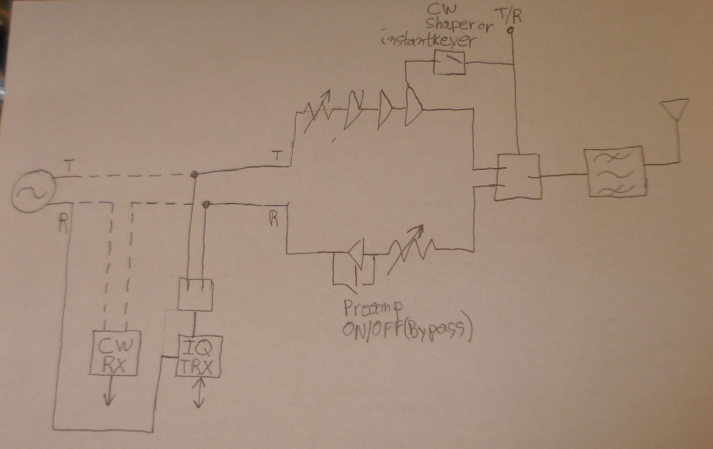
The picture
above shows how the oscillator is to be connected in direct conversion transceivers in
both modes of operation. The dotted lines are for connection of the
oscillator to a CW receiver. The continuous lines are for connection of
the oscillator to an I/Q transceiver (excluding its RF amplifiers). The RF power amplifier and
preamplifier sections are common to both modes of operation. Hopefully,
this diagram will show you how to properly connect your Super VFO to
the rest of your direct conversion transceiver.
The Super
VFO has been built in an ordinary metal project enclosure (it has to be
all metal, do not use plastic or any other non-metal material). On the
front panel, there is the ON/OFF switch, the TX/RX indicator LED, the
frequency and band controls and the RIT/Fine-frequency control. On the
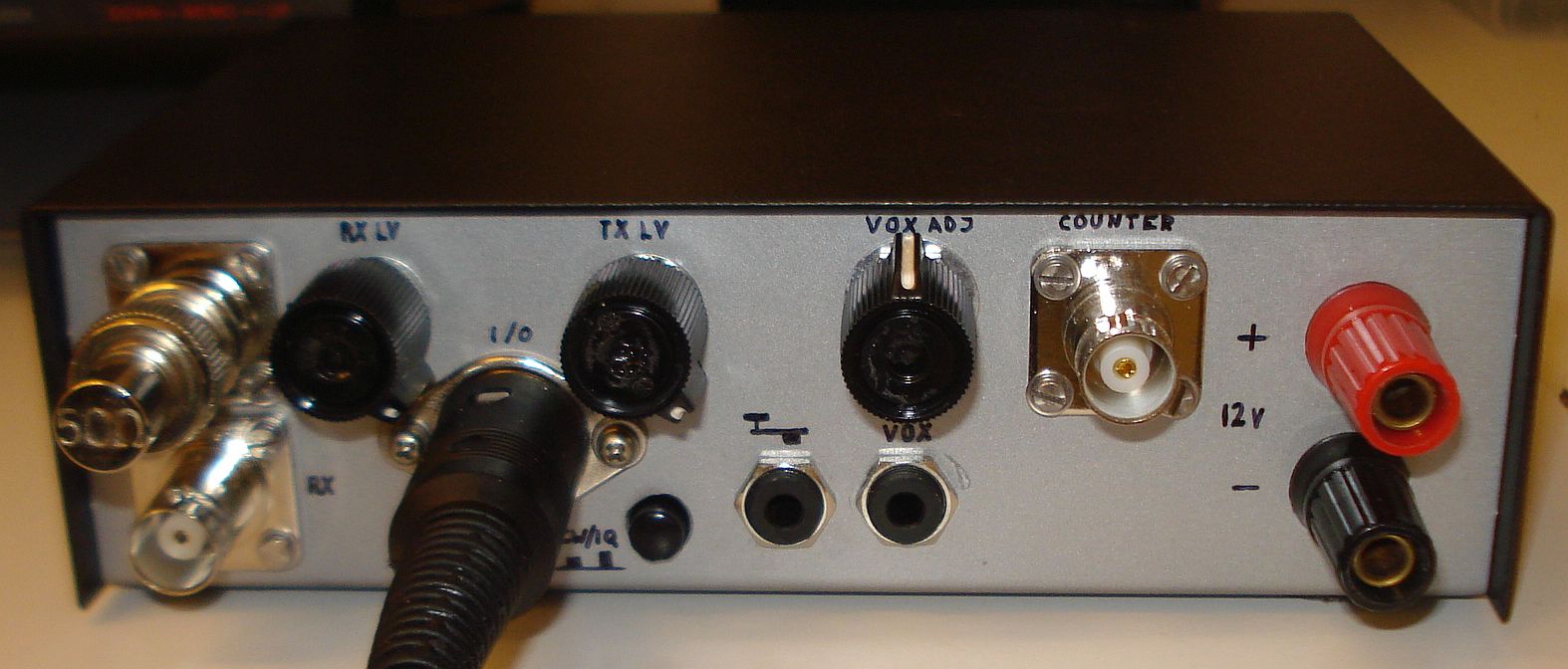
back panel, there is the RX and TX signal connectors and their signal
level potentiometers, the counter output connector, the DIN connector,
the mode switch, the external key connector, the VOX adjustment and
connector and of course the power connectors.
Near every control or connector, markings have been made, using a permanent marker. Markings are important, not only to make you remember what each knob or connector does, but also when you want your completed homebrew equipment to look more "commercial". It really makes a difference in the "look" of the equipment, so spend some time on it if you like good looking gear. The permanent marker is a good solution as it cannot be erased, unless you use alcohol or acetone. You can do really good markings with a steady hand and the help of some rulers. You can also use stencils for the various shapes and the letters (if you can find ones with small letters). Use your imagination to find out the best result. If you do not like it, you can erase it (or part of it) and then start all over again until you are satisfied. You can also use multiple color permanent markers if you like, either on the panel or on the knobs. For example, I used a white permanent marker, to draw some indexing lines and dots onto some black knobs that did not have any.
For the RF connectors, I used BNC ones. They do not need to be expensive varieties for HF. For the chassis I used these with the square flange, to prevent them form get un-screwed from the chassis. BNC connectors are an excellent choice. They are cheap, small (compared with UHF or N-type) they have the locking mechanism, they can be quickly inserted and locked or pulled out, they do not get un-screwed but they can be turned without disconnected. For the I/O signals connector I used the DIN type because it requires a circular hole on the chassis. A serial port or a VGA connector could have been used as well, but they require special holes for mounting.
UPDATE 16 Nov 2021
The next
version is an update from the previous one. This time I have replaced
the RIT in CW mode, with TIT (transmitter incremental tuning). This
removes fine tuning capability on RX but it adds a very important
feature, which is the "Spot" switch. By pressing this switch and zero
beating an incomming CW signal on RX mode, you automatically tune your
transmitter to this received signal. This is so useful in direct
conversion non-phasing receivers (which receive both sidebands), so
that you transmit at the right sideband and not the opposite one, of
that of the incoming RX signal. On I/Q mode, the spot switch has no
effect, and the fine tune is again available.